Background and Research Motivation
Relaxor ferroelectrics are a class of functional materials highly valued for their high dielectric permittivity and excellent electromechanical coupling, making them promising candidates for next-generation sensors, actuators, memory, and energy storage devices. However, their unique properties stem from complex, disordered atomic structures that have historically been challenging to characterize in three dimensions. Traditional techniques, such as X-ray diffraction and conventional electron microscopy, provide average structural information but struggle to map individual atomic irregularities in detail.
Key Findings and Methodology
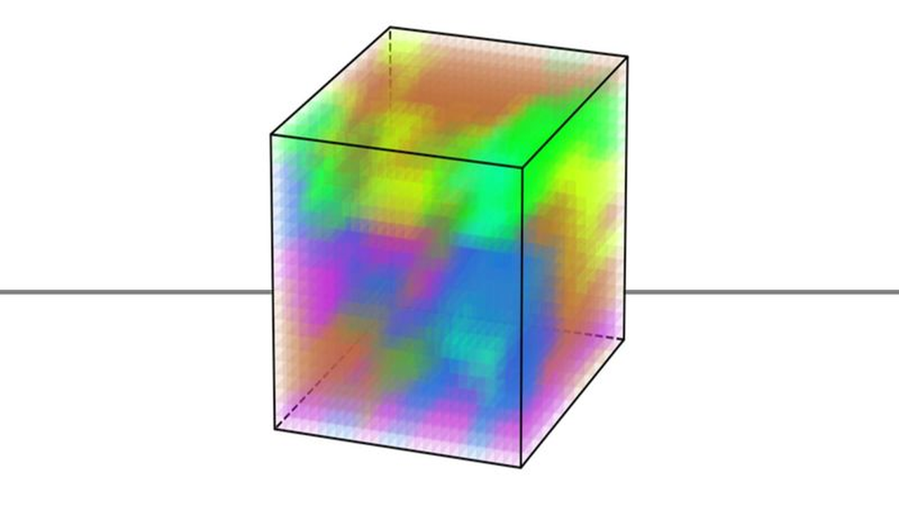
A research team at the Massachusetts Institute of Technology (MIT), in collaboration with other institutions, has made a significant breakthrough by applying advanced multi-slice electron ptychography (MEP) to relaxor ferroelectrics. MEP is a sophisticated imaging technique that precisely measures the phase and amplitude of electron waves transmitted through a sample, subsequently reconstructing its 3D atomic structure at the nanometer scale. This method allowed the researchers to reveal intricate patterns of localized polarization domains and atomic displacements within relaxor ferroelectrics with unprecedented clarity.
Specifically, the study sheds new light on how the relaxor behavior—where the dielectric response exhibits frequency dispersion depending on temperature or electric field—arises from subtle atomic structural irregularities. The resulting 3D atomic structure data, published in Science, provides foundational insights that will dramatically improve the accuracy of computational models used to predict the behavior of complex disordered materials.
Technical Significance and Outlook
This research is profoundly significant, not only deepening the fundamental scientific understanding of relaxor ferroelectrics but also directly impacting material design and application development. With high-resolution 3D atomic structure information now accessible, researchers can precisely engineer ferroelectric materials with specific functionalities from the atomic level. This advancement is expected to accelerate innovation in several application areas:
- High-Performance Sensors: Development of highly sensitive and responsive pressure, ultrasonic, and vibration sensors.
- High-Density Memory: Enhancement of low-power, non-volatile ferroelectric random-access memory (FeRAM) devices.
- Energy Devices: Realization of more efficient thermoelectric materials, capacitors, and energy harvesting technologies.
- Advancement in AI Materials Science: The acquired data will be invaluable for training machine learning models, thereby improving the accuracy of AI-driven new material discovery and property prediction.
This breakthrough opens new frontiers in functional materials research, laying a critical foundation for future electronic devices and energy technologies.








Comments