Background
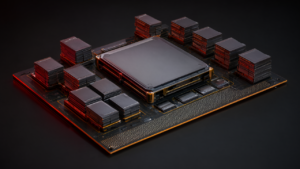
The exponential growth of AI workloads presents both significant challenges and opportunities for the semiconductor industry. Historically, data transfer speed and memory bandwidth limitations have emerged as major bottlenecks restricting chip performance. 2.5D packaging offers a critical solution by allowing multiple dies—such as High Bandwidth Memory (HBM) and logic processors—to be placed side-by-side on a silicon interposer. This technique facilitates shorter, denser electrical connections compared to traditional wire bonding or flip-chip methods, which in turn leads to a significant reduction in signal latency and power consumption. Advanced packaging solutions, including 2.5D, are now widely adopted in cutting-edge AI accelerators, High-Performance Computing (HPC) systems, and data center processors, as highlighted by reports such as one from Econ Market Research.
Key Findings
The adoption of HBM-integrated 2.5D packaging for AI accelerators is rapidly gaining momentum, with industry leaders TSMC and Samsung spearheading the technological innovation. TSMC’s CoWoS-S platform currently supports silicon interposers approximately 3.3 times the conventional reticle area, while its CoWoS-L variant is already in volume production at 3.5 times, with ambitious plans for further expansion to 5.5 times by 2026. Concurrently, Samsung’s I-CubeS platform supports configurations utilizing 6 HBM2E stacks and is actively developing solutions for 8-HBM3 arrangements, marking significant strides in high-performance computing capabilities.
Further technical advancements include:
- TSMC CoWoS Evolution: TSMC’s CoWoS-S (Chip-on-Wafer-on-Substrate) platform has demonstrated the integration of silicon interposers up to approximately 3.3 times the standard reticle size. This capability is paramount for establishing high-density connections between 4-8 HBM stacks and logic devices, a fundamental requirement for demanding AI training accelerators. The CoWoS-L platform has already achieved volume production at roughly 3.5 times the reticle size, with strategic plans to further expand to approximately 5.5 times by 2026. These significant expansions are vital, as escalating AI chip performance requirements necessitate progressively larger interposer areas and increased HBM capacity.
- Samsung I-CubeS Deployment: Samsung’s advanced packaging platform, I-CubeS, is a key contributor to this rapidly evolving domain. Current I-CubeS configurations are engineered to support 6 HBM2E stacks, with ongoing development for future architectures accommodating 8-HBM3 arrangements. Samsung has also successfully qualified interposer-based packages roughly 3.3 times the reticle size, thereby addressing the critical demands for high-bandwidth and large-memory integration in contemporary AI chips.
- HBM Criticality: The high-speed data transfer and massive processing capabilities required by modern AI, HPC, and data center processors inherently necessitate the use of 4-8 HBM stacks. These HBM stacks interface with logic devices through sophisticated silicon interposers or high-density redistribution layers (RDLs). This approach delivers superior bandwidth and enhanced power efficiency when compared to conventional packaging methods, making it indispensable for mitigating performance bottlenecks prevalent in intensive AI workloads.
Looking ahead, the ongoing evolution of 2.5D packaging and HBM integration by industry leaders TSMC and Samsung is set to propel AI chip performance to unprecedented levels. The drive towards larger reticle sizes and an increased number of HBM stacks is fundamental for addressing the colossal computational and data bandwidth demands anticipated from future AI models. Moreover, the growing adoption of open chiplet interconnect standards, such as UCIe 3.0, will further unlock new possibilities for integrating multi-vendor chiplets. This will enable the creation of even more complex, modular, and high-performing AI systems, pushing the frontiers of semiconductor manufacturing and fundamentally redefining computing for the AI era.
Source: https://www.econmarketresearch.com/blog/top-companies-in-advanced-semiconductor-packaging
Get our weekly technology intelligence — free
Receive an infographic that lets you judge at a glance whether each field’s analysis report is worth reading.
Subscribe Free — Weekly Tech Intelligence
By subscribing, you’ll receive Troy-Technical’s weekly technology intelligence newsletter.
- Your email and selected fields are used only to deliver the newsletter.
- We never share your information with third parties.
- You can unsubscribe anytime via the link in each email.
See our Privacy Policy for details.
Takes about a minute · Unsubscribe anytime