Key Findings
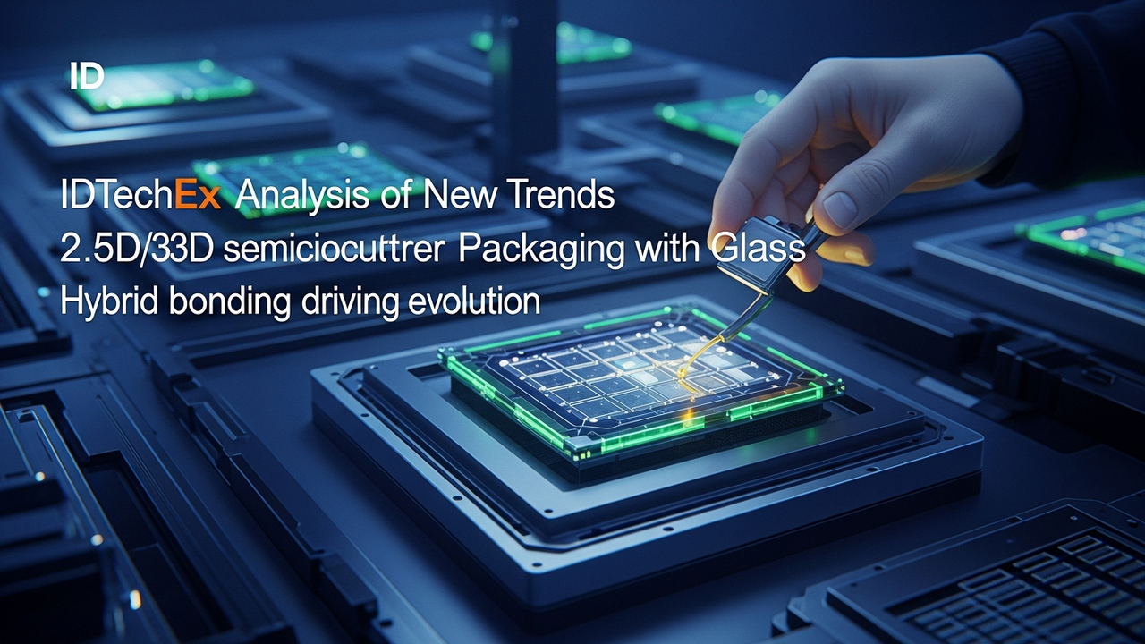
The latest analysis from IDTechEx emphasizes glass interposers and hybrid bonding technologies as key emerging trends in the evolution of semiconductor packaging. Glass interposers, compatible with panel-level packaging (PLP), hold significant promise for achieving high-density routing at a more manageable cost. Concurrently, hybrid bonding (copper-to-copper) for HBM (High Bandwidth Memory) is identified as an indispensable technology for enabling ultra-fine pitch vertical interconnections between chips. These technologies are accelerating the adoption of the chiplet concept and heterogeneous integration, vigorously driving the demand for advanced packaging solutions in critical markets such as High-Performance Computing (HPC), autonomous vehicles, and 5G communications.
Technical / Clinical Details
Glass interposers offer several advantages over traditional silicon interposers, including easier large-area scaling, superior electrical properties (low dielectric loss), and greater mechanical strength. Their coefficient of thermal expansion is intermediate between organic substrates and silicon, which helps mitigate thermal stress between dissimilar materials and improves reliability. This enables higher-density routing layers at potentially lower costs while ensuring high-frequency signal transmission quality. Compatibility with Panel Level Packaging (PLP) further contributes to potential cost reductions through economies of scale in manufacturing. Hybrid bonding (Cu-Cu bonding) is a technology that directly connects chiplets at pitches far finer than micro-bumps (sub-micron level). This dramatically increases I/O density, maximizes data bandwidth, and improves power efficiency. Especially in the integration of HBM with logic dies, this technology is critical for alleviating data movement bottlenecks and significantly boosting the performance of high-performance chips like AI accelerators. Chiplets and heterogeneous integration enhance design flexibility, improve yield, and facilitate system customization by optimally integrating multiple chips with different functionalities.
Background & Context
The limitations of Moore’s Law and the escalating demand from compute-intensive applications such as AI, HPC, and autonomous driving are compelling the semiconductor industry to explore new avenues for performance improvement. As transistor miniaturization alone becomes more challenging for performance gains, advanced packaging technologies have emerged as the primary means to drive system-level performance enhancements. Technologies like glass interposers and hybrid bonding are at the forefront of this paradigm shift, aimed at overcoming the limitations of conventional packaging. These advancements are spurring massive investments and technological development across the entire semiconductor supply chain, creating new business opportunities for material suppliers, manufacturing equipment vendors, and design service providers.
Strategic Significance & Outlook
Glass interposers and hybrid bonding are expected to play increasingly vital roles in the 2.5D/3D semiconductor packaging market over the next few years. The widespread adoption of these technologies will dramatically enhance the performance of AI accelerators, next-generation data centers, automotive AI platforms, and 5G/6G infrastructure. As mass production techniques for glass interposers mature and hybrid bonding becomes more standardized, more complex and higher-performance chiplet-based systems are anticipated to be developed and manufactured more cost-effectively. These trends will be central to reshaping the competitive landscape of the semiconductor industry and generating a new wave of technological innovation.
Get our weekly technology intelligence — free
Receive an infographic that lets you judge at a glance whether each field’s analysis report is worth reading.
Subscribe Free — Weekly Tech Intelligence
By subscribing, you’ll receive Troy-Technical’s weekly technology intelligence newsletter.
- Your email and selected fields are used only to deliver the newsletter.
- We never share your information with third parties.
- You can unsubscribe anytime via the link in each email.
See our Privacy Policy for details.
Takes about a minute · Unsubscribe anytime