Background
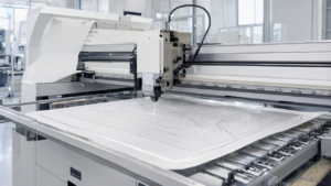
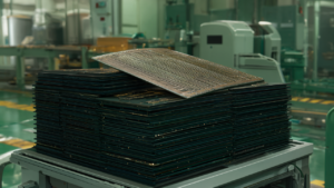
The relentless evolution of artificial intelligence necessitates increasingly rapid and voluminous data processing, fueling an explosive demand for GPUs, AI accelerators, and their supporting High Bandwidth Memory (HBM). Historically, front-end miniaturization was the primary driver for performance gains in semiconductor manufacturing. However, this approach is now encountering significant technological limits and escalating costs. In response, advanced packaging – the efficient integration of multiple chips – has rapidly emerged as a crucial new frontier for enhancing performance and achieving cost reductions. This paradigm shift is dramatically elevating the importance of backend equipment investment within the broader semiconductor manufacturing ecosystem.
Key Findings
Applied Materials has announced a substantial upgrade to its 2026 advanced packaging business revenue growth forecast, elevating it from “over 50%” to “over 70%.” This significant revision decisively signals a rapid expansion of AI semiconductor investments beyond traditional front-end process miniaturization, now extending into critical backend domains like High Bandwidth Memory (HBM) and complex multi-layer packaging. Advanced packaging is paramount for integrating multiple chips to achieve the higher performance and efficiency essential for next-generation AI capabilities.
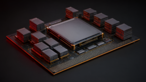
Specifically, HBM stacking, which involves vertically integrating DRAM chips to dramatically boost bandwidth, necessitates sophisticated die bonding, thermo-compression bonding (TCB), and precision inspection equipment. Applied Materials’ equipment provides key technologies essential for these complex stacking processes and heterogeneous integration, suggesting its deep integration within the mainstream advanced packaging technologies driving the AI era.
However, a critical new constraint on customer capital expenditure has emerged: securing adequate cleanroom space. This cleanroom bottleneck, alongside other infrastructure limitations, indicates that the scaling of AI semiconductor production is hindered not just by equipment supply but also by the need for significant infrastructure investment in advanced manufacturing environments, demanding a more balanced investment approach across the entire semiconductor ecosystem. Applied Materials’ strong forecast underscores a sustained structural expansion of the AI semiconductor market, positioning the company to maximize benefits from its technological leadership, even as industry-wide infrastructure constraints require strategic investment and collaboration across the backend supply chain to meet future AI demands.
Source: https://xenospectrum.com/en/applied-materials-packaging-growth/
Get our weekly technology intelligence — free
Receive an infographic that lets you judge at a glance whether each field’s analysis report is worth reading.
Subscribe Free — Weekly Tech Intelligence
By subscribing, you’ll receive Troy-Technical’s weekly technology intelligence newsletter.
- Your email and selected fields are used only to deliver the newsletter.
- We never share your information with third parties.
- You can unsubscribe anytime via the link in each email.
See our Privacy Policy for details.
Takes about a minute · Unsubscribe anytime