Key Findings
Intel has forged a pivotal collaboration with Lens Technology, a company renowned for its proficiency in glass materials, high-precision laser processing, and advanced manufacturing capabilities. This strategic alliance is aimed at significantly accelerating innovation in advanced semiconductor packaging technologies, which are increasingly critical for meeting the demanding requirements of the artificial intelligence (AI) era.
Technical / Clinical Details
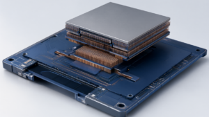
The partnership will integrate Lens Technology’s deep expertise in developing novel glass substrates and its ultra-precise laser processing techniques with Intel’s advanced semiconductor designs. Glass substrates offer superior electrical performance, enhanced thermal dissipation, and structural rigidity compared to traditional organic substrates, enabling higher interconnect densities and finer pitch features in advanced packaging. This allows for the creation of more compact, power-efficient, and higher-performing AI chipsets and other high-performance computing components. Such advancements are essential for enabling chiplet architectures and 3D stacking, driving breakthroughs in power, performance, and form factor for next-generation AI infrastructure.
Background & Context
As the semiconductor industry pushes beyond the limits of Moore’s Law, advanced packaging has emerged as a crucial frontier for continued performance scaling and integration. Technologies like 2.5D/3D packaging and heterogeneous integration are vital for connecting multiple chiplets and functionalities within a single package, improving overall system performance and energy efficiency. Intel’s collaboration with a materials and manufacturing specialist like Lens Technology underscores the industry-wide recognition that innovation in packaging materials and processes is paramount for the future of computing, especially for data-intensive applications like AI.
Strategic Significance & Outlook
This collaboration is expected to yield significant advancements in the foundational technologies that underpin AI hardware. The resulting innovations in advanced packaging will enable the deployment of more powerful and efficient AI-enabled semiconductors across a wide array of applications, from data centers and edge computing to autonomous systems. By combining their strengths, Intel and Lens Technology aim to provide global customers with state-of-the-art AI-ready silicon, thereby contributing substantially to the evolution and expansion of the global AI ecosystem and maintaining a competitive edge in a rapidly evolving technological landscape.
Get our weekly technology intelligence — free
Receive an infographic that lets you judge at a glance whether each field’s analysis report is worth reading.
Subscribe Free — Weekly Tech Intelligence
By subscribing, you’ll receive Troy-Technical’s weekly technology intelligence newsletter.
- Your email and selected fields are used only to deliver the newsletter.
- We never share your information with third parties.
- You can unsubscribe anytime via the link in each email.
See our Privacy Policy for details.
Takes about a minute · Unsubscribe anytime