Key Findings
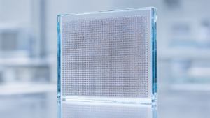
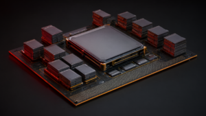
As AI chips increasingly demand larger and more complex packages, the development race for glass substrates as a next-generation packaging material is intensifying. In this competitive landscape, Japan’s Shinko Electric Industries has successfully developed a 22-layer glass substrate, featuring 11 copper wiring layers laminated on each side of the glass core. This significant technological breakthrough directly addresses a major challenge in multi-layer glass substrate manufacturing: internal cracking and delamination, commonly referred to as the SeWaRe issue. Shinko Electric Industries showcased this cutting-edge glass core substrate at the Advanced Packaging Summit 2026 in July, demonstrating its advanced technological capabilities to the global industry.
Technical Details
Multi-layer glass substrates are essential for achieving the high-density interconnections required by AI chips. However, a significant challenge arises from the tendency for internal stresses, caused by laminating multiple layers of materials with different coefficients of thermal expansion, to induce cracks and delamination. Shinko Electric Industries’ 22-layer glass substrate is believed to incorporate proprietary material design and process technologies to overcome this SeWaRe issue. Key aspects likely include careful selection of the glass core, optimization of material compatibility between copper wiring layers and dielectric layers, and precise control of temperature profiles and pressure during lamination. This allows for the production of highly reliable package substrates that maintain excellent dimensional stability and electrical properties, delivering the high bandwidth and low power loss necessary for advanced AI chips. Glass substrates also offer superior surface flatness compared to existing organic substrates, benefiting fine-pitch wiring pattern formation and precise chiplet placement.
Background & Context
High-performance AI processors increasingly adopt 2.5D/3D packaging that integrates numerous chiplets, including High-Bandwidth Memory (HBM). Such complex structures demand substrates with exceptional thermal stability, signal integrity, and mechanical strength. Conventional organic substrates are nearing their limits in terms of warpage and wiring density, hindering further evolution of AI chips. Glass substrates are emerging as a promising solution to these challenges, with major players like Intel and SKC also intensifying their development efforts, leading to vibrant global technological competition. Shinko Electric Industries’ latest achievement, particularly in multi-layer technology, demonstrates Japan’s strong competitive edge in materials technology, reinforcing Japan’s role in the next-generation AI chip supply chain.
Strategic Significance & Outlook
Shinko Electric Industries’ success with the 22-layer glass substrate marks a significant step towards the mass production of glass substrates. This development is expected to drive broader adoption of glass substrates in AI chips, further enhancing the performance and efficiency of AI computing. Future efforts will likely focus on reducing manufacturing costs, improving production throughput, and developing even higher-layer count and finer-pitch technologies. As reports suggest Samsung Electro-Mechanics faces ramp-up uncertainties, the manufacturing of glass substrates demands highly advanced technology and significant capital investment, implying that technologically leading companies will drive the market. Glass substrates hold the potential to establish a new standard for semiconductor packaging in future AI data centers, edge AI, and high-performance mobile devices.
Get our weekly technology intelligence — free
Receive an infographic that lets you judge at a glance whether each field’s analysis report is worth reading.
Subscribe Free — Weekly Tech Intelligence
By subscribing, you’ll receive Troy-Technical’s weekly technology intelligence newsletter.
- Your email and selected fields are used only to deliver the newsletter.
- We never share your information with third parties.
- You can unsubscribe anytime via the link in each email.
See our Privacy Policy for details.
Takes about a minute · Unsubscribe anytime