Key Findings
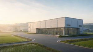
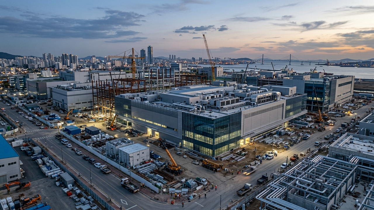
HANMI Semiconductor has announced the establishment of its largest-ever 8th production facility, a substantial investment totaling $91.4 million (approximately 130 billion Korean Won), through the acquisition of Mercury Co., Ltd.’s factory in Incheon’s Puan National Industrial Complex. This initiative is a proactive response to the persistent global shortage of AI semiconductor equipment. The new facility is slated to begin mass production in Q2 2027 and will focus on manufacturing next-generation advanced semiconductor equipment. This includes TC bonders for High-Bandwidth Memory (HBM), hybrid bonders, 2.5D packaging equipment for AI semiconductors, and BOC COB bonders for high-performance memory production.
Technical Details
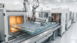
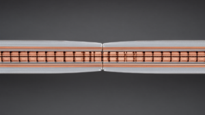
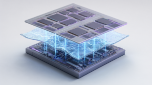
TC (Thermo-Compression) bonders for HBM are crucial for precisely joining multiple DRAM dies vertically, leveraging heat and pressure. This technology is essential for achieving the high bandwidth and low latency characteristic of HBM and supports advanced connection techniques like micro-bumping and hybrid bonding. Hybrid bonders enable finer-pitch die-to-die connections, such as copper-to-copper direct bonding, enhancing electrical performance and thermal conductivity. Furthermore, 2.5D packaging equipment for AI semiconductors supports processes like CoWoS (Chip-on-Wafer-on-Substrate), which integrates GPUs or ASICs with HBM on a silicon interposer. BOC COB bonders contribute to the production of more robust and reliable high-performance memory packages, supporting the high-speed and stable data processing capabilities indispensable for AI workloads.
Background & Context
The demand for AI chips is surging across diverse sectors, including data centers, edge AI, and autonomous driving, dramatically elevating the importance of HBM and advanced packaging technologies. New technical challenges are emerging that traditional semiconductor manufacturing equipment cannot adequately address, increasing expectations for back-end equipment manufacturers like HANMI Semiconductor. HANMI Semiconductor’s substantial investment strategically responds to these market trends, fundamentally strengthening its capacity to supply equipment critical for AI-era foundational technologies such as HBM and 2.5D/3D packaging. This aligns with South Korea’s national strategy to maintain a leading role in the global semiconductor supply chain, particularly in memory and advanced packaging.
Strategic Significance & Outlook
Once the new Incheon production facility commences mass production in Q2 2027, HANMI Semiconductor will significantly expand its supply capacity in the HBM and advanced packaging equipment markets, thereby bolstering its global competitiveness. This investment is expected to help alleviate bottlenecks faced by AI semiconductor manufacturers, fostering further innovation and widespread adoption of AI technology. In the future, with the proliferation of hybrid bonding and other next-generation packaging technologies, HANMI Semiconductor’s equipment will become key to realizing more highly integrated and high-performance AI systems. This will contribute to improved data center efficiency, the development of new AI applications, and the sustained growth of the entire semiconductor ecosystem.
Get our weekly technology intelligence — free
Receive an infographic that lets you judge at a glance whether each field’s analysis report is worth reading.
Subscribe Free — Weekly Tech Intelligence
By subscribing, you’ll receive Troy-Technical’s weekly technology intelligence newsletter.
- Your email and selected fields are used only to deliver the newsletter.
- We never share your information with third parties.
- You can unsubscribe anytime via the link in each email.
See our Privacy Policy for details.
Takes about a minute · Unsubscribe anytime