Background
The semiconductor industry is actively confronting the limitations of Moore’s Law, increasingly looking to next-generation devices based on 2D materials like graphene to address persistent challenges in performance enhancement and energy efficiency. However, a major long-standing hurdle has been the seamless integration of these novel materials into existing CMOS manufacturing processes for high-volume, high-quality production. Historically, critical bottlenecks for industrialization included controlling material defects, achieving uniform doping, and ensuring reproducibility at the wafer level. This groundbreaking research significantly resolves many of these key bottlenecks, transforming the potential for 2D materials to drive the future of the electronics industry into a tangible reality.
Key Findings
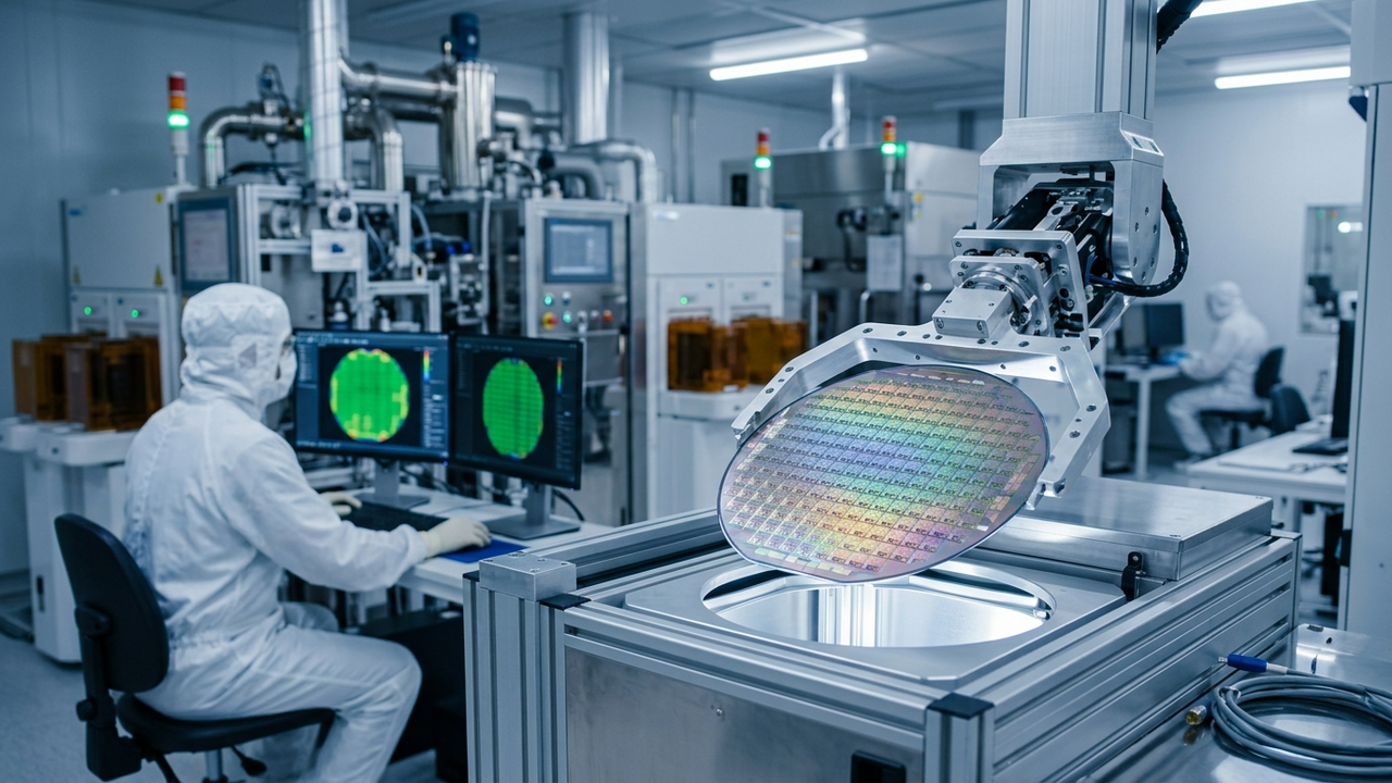
Researchers have successfully optimized both the manufacturing and analysis processes for CMOS-compatible graphene field-effect transistors (GFETs) on 200 mm wafers. This represents a significant stride towards industrial application within a pilot-line environment. The optimized process demonstrates an exceptionally high device yield of 97%, complemented by excellent doping uniformity, low contact resistance, and high carrier mobility.
Technical Details
The study encompassed innovative optimization across multiple crucial steps of GFET manufacturing. This included advancements in graphene layer transfer techniques, gate dielectric formation, electrode bonding, and patterning processes. The ability to manufacture GFETs on relatively large 200mm wafers is particularly significant, as it demonstrates high compatibility with existing semiconductor fabrication lines, thereby substantially reducing the barriers to mass production. The achieved 97% device yield is critically important for ensuring the cost-efficiency and reliability required for commercial production. Moreover, the excellent doping uniformity guarantees consistent device performance, while the demonstrated low contact resistance and high mobility strongly suggest that GFETs possess the potential to outperform traditional silicon-based devices in demanding high-frequency, high-speed, and low-power consumption applications.
Strategic Significance & Outlook
The successful optimization of GFET manufacturing processes on 200mm wafers establishes a robust foundation for the widespread adoption of graphene-based devices across a broad spectrum of applications. These include critical sectors such as IoT, 5G/6G communications, artificial intelligence, and high-performance computing. Further advancements in this technology, particularly its expansion to larger 300mm wafers, could position graphene devices to complement or even partially replace silicon technology, thereby unlocking significant new growth opportunities for the electronics industry. Both investors and semiconductor manufacturers are keenly observing the long-term impact and considerable commercial value that this breakthrough is poised to deliver.
Get our weekly technology intelligence — free
Receive an infographic that lets you judge at a glance whether each field’s analysis report is worth reading.
Subscribe Free — Weekly Tech Intelligence
By subscribing, you’ll receive Troy-Technical’s weekly technology intelligence newsletter.
- Your email and selected fields are used only to deliver the newsletter.
- We never share your information with third parties.
- You can unsubscribe anytime via the link in each email.
See our Privacy Policy for details.
Takes about a minute · Unsubscribe anytime









Comments