Key Findings
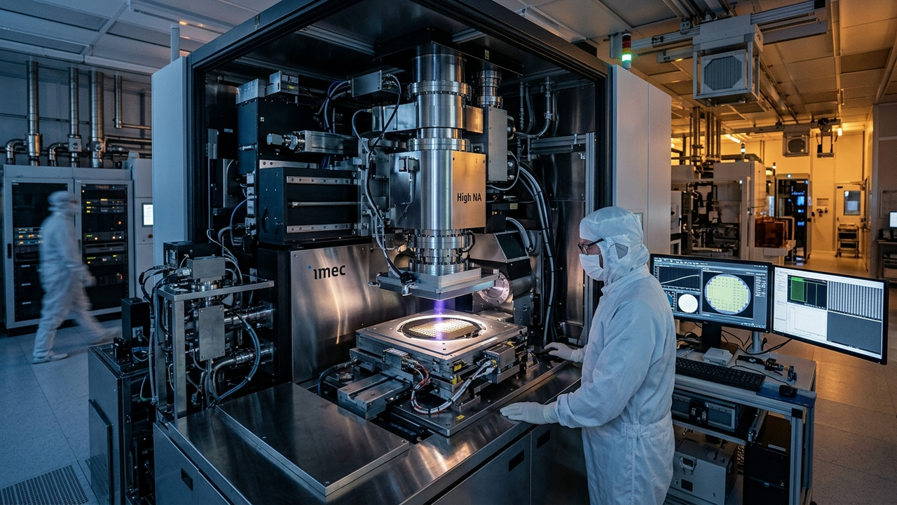
Imec has achieved a significant breakthrough in nanoelectronics research: an extension of chemically amplified resists (CARs) optimized for High Numerical Aperture Extreme Ultraviolet (High NA EUV) lithography. This innovative technology enables the formation of 22-nanometer (nm) pitch line structures using single patterning, substantially advancing current microchip manufacturing capabilities. This development marks a critical stride towards producing smaller, faster, more cost-effective, and environmentally sustainable next-generation microchips.
Technical Details
Extreme Ultraviolet (EUV) lithography stands as the state-of-the-art technology in contemporary semiconductor manufacturing, with High NA EUV specifically designed to deliver superior resolution compared to conventional EUV systems. However, continued miniaturization demands the concurrent development of highly compatible resist materials. Chemically Amplified Resists (CARs) utilize post-exposure chemical reactions to boost sensitivity and resolution, yet further performance enhancements were crucial to meet the stringent requirements of High NA EUV. Imec’s announced extension signifies that exceptionally fine 22nm line-and-space (L/S) patterns can now be consistently formed with a single exposure step.
- 22nm Pitch Achievement: This breakthrough fully leverages the high-resolution capabilities of High NA EUV lithography, enabling significantly higher integration density and performance advancements for next-generation DRAM, NAND flash memory, and high-performance logic chips.
- Single Patterning: In contrast to complex multi-patterning processes, this innovation dramatically simplifies manufacturing steps, leading to reduced production costs, increased throughput, and lower defect rates.
- Enhanced Sustainability: The inherent efficiency gains from simplified manufacturing translate to reduced energy consumption and optimized material usage, directly supporting the semiconductor industry’s critical initiatives to minimize its environmental footprint.
This technology is poised to directly enhance the performance across a vast spectrum of electronic devices, ranging from consumer smartphones and enterprise data center servers to advanced AI processors.
Background & Industry Context
The semiconductor industry is locked in an unrelenting pursuit of miniaturization and performance enhancement. Sustaining Moore’s Law, which predicts the doubling of transistors on an integrated circuit every two years, critically depends on continuous innovation in lithography technology. High NA EUV lithography is a cornerstone technology that major semiconductor manufacturers such as Intel, TSMC, and Samsung intend to deploy for their future advanced process nodes. Historically, the performance limitations of resist materials have represented a significant bottleneck for its practical implementation. Imec has actively collaborated with key industry players to overcome this formidable challenge. This latest achievement underscores the vital role of research institutions like imec in serving as pivotal hubs that bridge fundamental research with applied development within the broader semiconductor ecosystem.
Strategic Significance & Outlook
Imec’s recent announcement significantly accelerates the maturity of High NA EUV lithography technology, carrying profound implications for the semiconductor industry roadmap. The successful demonstration of single patterning at a 22nm pitch provides a clear pathway for the development of future extreme process nodes, such as 1.8nm and 1.4nm. Should this technology transition to high-volume manufacturing, it is anticipated to drive substantial performance enhancements and cost-efficiency improvements across diverse sectors, spanning from advanced consumer electronics to robust enterprise systems. Nanoelectronics research is thus poised to maintain its central role in driving the relentless evolution of the microchips that form the foundational backbone of our modern information society.
Source: https://www.imec-int.com/en
Get our weekly technology intelligence — free
Receive an infographic that lets you judge at a glance whether each field’s analysis report is worth reading.
Subscribe Free — Weekly Tech Intelligence
By subscribing, you’ll receive Troy-Technical’s weekly technology intelligence newsletter.
- Your email and selected fields are used only to deliver the newsletter.
- We never share your information with third parties.
- You can unsubscribe anytime via the link in each email.
See our Privacy Policy for details.
Takes about a minute · Unsubscribe anytime









Comments