Key Findings
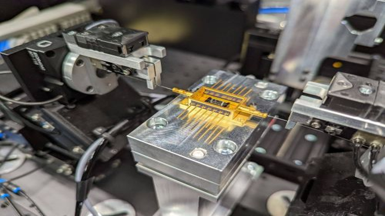
An industry meeting hosted by Optica Online in June 2026 will spotlight advanced photonic packaging technologies crucial for scaling photonic systems across AI infrastructure, datacom, sensing, and quantum applications. The discussions will delve into essential techniques such as heterogeneous integration, wafer-level testing, fiber attach, thermal management, and co-packaged optics (CPO), all vital for transitioning from prototyping to mass production. This initiative aims to identify and resolve critical bottlenecks in the industrialization of photonics, opening doors for its broader application in various industries.
Technical / Clinical Details
- Heterogeneous Integration: This technology, which integrates multiple chips and components manufactured with different materials or processes into a single package, is indispensable for performance enhancement and miniaturization.
- Wafer-Level Testing: Testing photonic devices early in the manufacturing process helps reduce defects and improve cost efficiency.
- Fiber Attach: The precise and efficient attachment of optical fibers to photonic chips is paramount for minimizing signal loss.
- Thermal Management: Effective dissipation of heat generated by densely integrated photonic systems ensures stable operation and extended device lifespan.
- Co-Packaged Optics (CPO): Integrating electro-optical conversion elements directly within the same package as CPUs or GPUs dramatically increases bandwidth and reduces power consumption.
These technologies are crucial for meeting the explosive data processing demands and energy efficiency challenges in AI data centers. Large-scale AI training and inference require ultra-high-speed, low-latency interconnects unattainable with conventional electrical wiring, making photonic packaging a promising solution.
Background & Context
The photonics industry is experiencing unprecedented attention, largely driven by the rapid expansion of AI infrastructure that demands high-speed data transfer and energy efficiency. Major players like Nvidia, Broadcom, and Marvell are intensely competing on electrical/thermal efficiency. Advanced packaging technologies are central to unlocking the full potential of photonic integrated circuits (PICs), simultaneously bolstering supply chains and promoting ‘reshoring’ initiatives. European efforts such as PhotonDelta exemplify the robust support for technological development and industrialization in this field.
Strategic Significance & Outlook
The technological advancements discussed at this meeting underscore photonics’ role as a foundational scaling layer for AI-era computing. CPO, in particular, is key to resolving GPU communication bottlenecks caused by increasing data center traffic, striving for the ‘ultimate goal’ of low latency and reduced power consumption. As these technologies mature and become viable for mass production, innovation will accelerate across a wide range of applications, including LiDAR sensors for autonomous vehicles, quantum computing systems, and advanced sensing platforms. Photonics is poised to become a central driver of the next wave of technological innovation.
Source: https://www.optica.org/events/webinar/2027/october/advanced_packaging_for_photonics/


Comments