Background
Semiconductor technology is confronting the physical limits of Moore’s Law, shifting focus from traditional miniaturization strategies to advanced packaging techniques like 3D stacking and heterogeneous integration. Fusion bonding is a foundational technology for directly connecting different wafers or dies in the formation of chiplets and 3D ICs, with its precision directly correlating to final product performance and yield. Particularly in innovative architectures such as Backside Power Delivery Networks (BSPDN), ultra-high-precision bonding is required between the device layer and the power delivery layer. Conventional bonding techniques face challenges where minor distortions introduced during bonding can compromise the exposure accuracy in subsequent lithography, leading to reduced yield and increased manufacturing costs. The current research provides an effective solution to these challenges, accelerating the mass production of next-generation semiconductors.
Key Findings
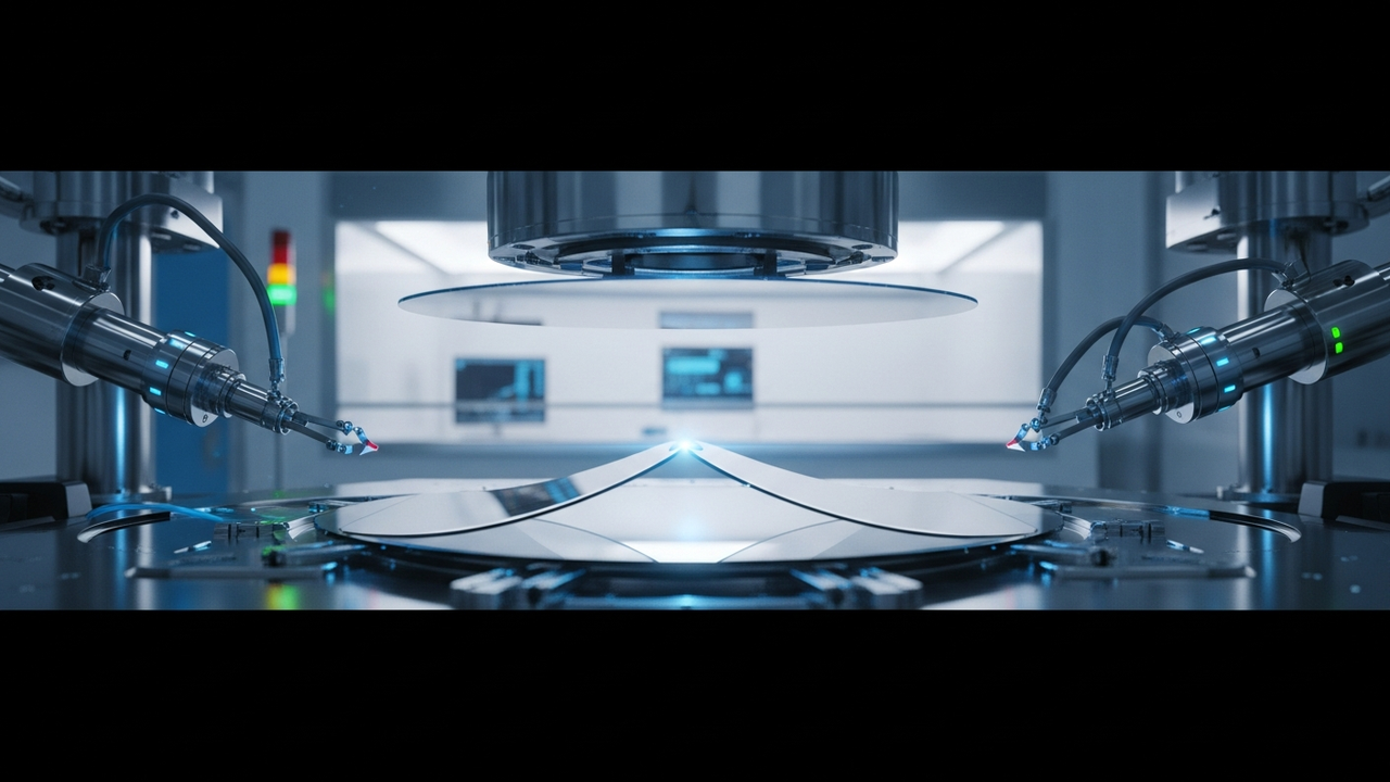
In recent research, an innovative method has been developed to significantly suppress distortion during the fusion bonding process by precisely curving wafers pneumatically. This technique achieves an exceptionally low residual grid distortion of less than 10 nanometers in bonded wafers, holding the potential to dramatically improve the precision and yield of next-generation semiconductor manufacturing processes.
Technical Details
This novel fusion bonding approach precisely imparts curvature to wafers within a pneumatic chamber *before* direct bonding, effectively distributing and mitigating stress concentrations during the joining process. Traditional fusion bonding often leads to shape deformation and localized stress due to subtle wafer misalignments and thermal history, which can cause alignment errors and circuit defects in subsequent lithography steps. By contrast, this pneumatic curving technique achieves uniform bonding across the entire wafer, resulting in low distortion that does not adversely affect downstream processes. A residual grid distortion of less than 10 nanometers signifies near-atomic layer precision, a critical achievement for advanced structures like Backside Power Delivery Networks (BSPDN) which incorporate high-density wiring layers on the wafer’s backside.
BSPDN is gaining significant attention as a technology that drastically improves the power efficiency and performance of high-performance computing (HPC) and AI accelerators by enhancing power delivery efficiency and reducing signal noise in semiconductor chips. For BSPDN, where fine power delivery layers are formed on the wafer’s backside, even slight distortion in the bonding layer can severely degrade the accuracy of subsequent lithography (patterning), directly impacting yield. The results of this study represent a groundbreaking advance in ensuring the reliability and scalability of fusion bonding for ultra-precise manufacturing processes such as BSPDN. This research is scheduled to appear in the proceedings of the IEEE ECTC 2026 (Electronic Components and Technology Conference), where it is anticipated to draw considerable interest from the semiconductor packaging community.
Implications & Outlook
This low-distortion fusion bonding technology is poised to significantly advance the practical implementation of Backside Power Delivery Networks (BSPDN), playing a crucial role in enhancing the power efficiency and performance of AI and HPC chips. Sub-10nm distortion control will enable the sustained accuracy of lithography in future, even finer nodes and multi-layered 3D IC structures, thereby increasing the robustness of manufacturing processes. Widespread adoption of this technology within the semiconductor industry is expected to contribute to improved yields and cost reduction in advanced packaging, accelerating the proliferation of high-performance semiconductors. Furthermore, this achievement will foster the continued development of precise stress management techniques in wafer-level manufacturing, strengthening the foundation for next-generation semiconductor fabrication as a whole.
Source: https://arxiv.org/abs/2606.04625


Comments