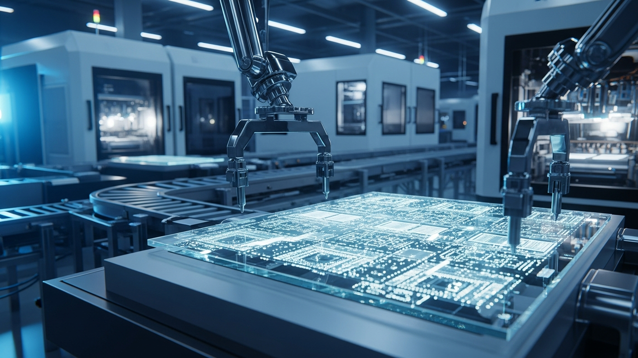
The Next Frontier in AI Packaging: Glass Substrates
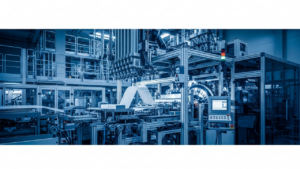
In advanced packaging technologies designed to push the limits of AI chip performance, glass substrates are emerging as the next-generation key material, accelerating an international development race towards their mass production. Glass overcomes the limitations of conventional organic substrates and silicon interposers, enabling higher-density and higher-performance chip integration, thus becoming an indispensable element for the evolution of AI and High Performance Computing (HPC) applications.
Unlocking Performance: Technical Advantages of Glass
Glass substrates surpass traditional materials in several critical aspects. Firstly, their exceptional dimensional stability enables extremely fine wiring pitches (sub-micron level) and high-density interconnections. This is essential for precisely integrating numerous chiplets and High Bandwidth Memory (HBM) within a single package. Secondly, an excellent Coefficient of Thermal Expansion (CTE) reduces thermal mismatch with the chips, thereby improving overall package reliability and thermal management performance. Furthermore, glass offers superior high-frequency characteristics, ensuring signal integrity crucial for the high-speed data transmission required by AI chips.
Global Race to Mass Production: Key Players and Investments
Intel has already invested over $1 billion in glass substrate research and development, unveiling its first samples combining Embedded Multi-die Interconnect Bridge (EMIB) packaging with glass core substrates at NEPCON Japan in January 2026. TSMC is also developing its CoPoS (Chip-on-Substrate-on-Package) technology, which utilizes glass core substrates and interposers, aiming for mass production in 2028-2029. Samsung is similarly advancing glass substrate technology as part of its vertical integration strategy, while SK Absolics, supported by the U.S. CHIPS Act, is constructing a dedicated factory in Georgia, targeting the start of glass substrate mass production by 2026. Chinese firms are also entering the fray; Visionox is leveraging its expertise in ultra-thin glass (UTG) and display panel manufacturing know-how to apply it to semiconductor-grade glass substrates. PCB manufacturer AKM Meadville established a pilot production line for glass substrates in January 2026 and has begun process verification.
Industry Context and Overcoming Current Limitations
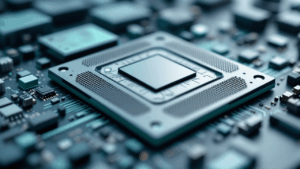
As AI chip designs grow increasingly complex, with chiplet architectures and 3D/2.5D integration becoming mainstream, the importance of packaging has escalated dramatically. Conventional organic substrates have faced limitations in miniaturization, warpage, and thermal management. While silicon interposers offer high performance, they are constrained by cost and size. Glass substrates are positioned as an ‘intermediate solution’ between these two, considered essential for enhancing the performance of next-generation HBM stacks, AI accelerators, and Co-Packaged Optics (CPO). Shortages of specific glass materials, such as low-CTE T-glass cloth, are exacerbating existing bottlenecks in the ABF (Ajinomoto Build-up Film) substrate market, making the securing of in-house production capabilities and supply chains for glass substrates an urgent priority for companies.
Outlook: Redefining Semiconductor Manufacturing
The global competition toward mass production of glass substrates will redefine the future of semiconductor packaging technology. As this technology matures, it promises significant improvements in AI chip performance, power efficiency, and cost-effectiveness, accelerating the realization of next-generation AI-driven devices and data centers. The substantial investments by leading semiconductor companies and specialized material manufacturers clearly indicate that glass substrates are not merely a research-phase technology but are poised to become mainstream in semiconductor manufacturing within a few years. This is expected to usher the semiconductor industry into a new phase of growth, strengthening the foundation for further innovation in AI technology.


Comments