Key Findings
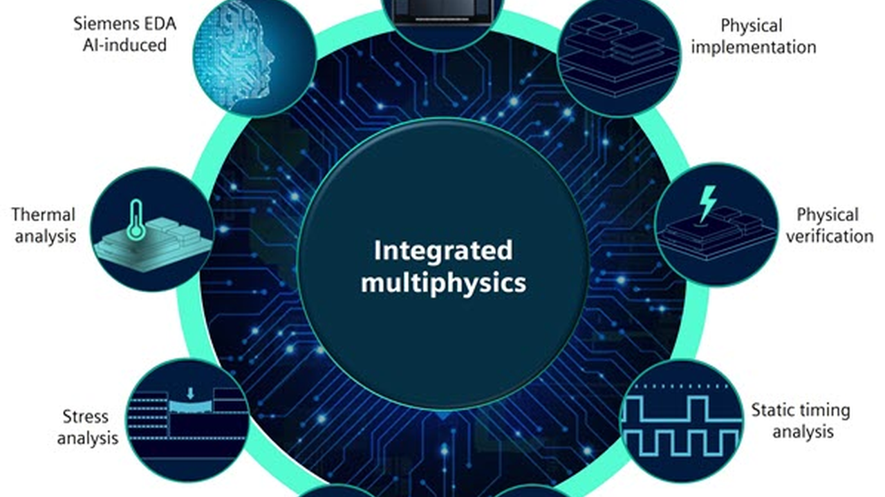
As the semiconductor industry shifts from conventional 2D integrated circuits to more advanced 2.5D and 3D-IC configurations, the associated verification complexity has dramatically increased. To overcome this challenge, multiphysics analysis is highlighted as indispensable for comprehensively evaluating thermal management, mechanical stress interactions, and extensive reliability verification requirements.
Technical Details
2.5D and 3D-IC packages achieve performance improvements and miniaturization by vertically or horizontally stacking and integrating multiple chips. However, this introduces complex interactions between various physical phenomena, such as thermal loads, mechanical stresses, and electromagnetic interference, experienced not only by individual chips but by the entire package. Multiphysics analysis is a powerful technique that simultaneously simulates the interactions between these different physical domains (thermal, structural, electrical). This enables the pre-identification of potential reliability issues that might be overlooked by single-physics models.
The article specifically discusses the impact of the following elements on assembly-level stress distribution and device characteristics:
- Die-Attach Materials: Materials used to fix chips to the package substrate; their elastic modulus and coefficient of thermal expansion (CTE) significantly influence stress distribution during thermal cycling.
- Underfill Properties: Materials filling the gap between the chip and substrate in packages like flip-chips and COWOS (Chip on Wafer on Substrate). Their CTE, elastic modulus, and adhesion directly impact stress relief and connection reliability.
- Package Substrates: The substrate that houses the chip and provides external connections. Its material properties and structure affect the overall package rigidity, thermal conduction, and stress transfer.
The selection and design of these materials are crucial for the long-term reliability of devices, particularly in preventing thermal-induced fatigue failure and delamination.
Background and Industry Context
The evolution of next-generation technologies like AI, High-Performance Computing (HPC), and 5G communication continues to push the performance limits of semiconductor chips. To meet these demands, as wiring miniaturization approaches its physical limits, semiconductor manufacturers are focusing on “More than Moore” approaches such as 2.5D/3D-ICs. However, this increase in integration density creates new, complex challenges in design, including thermal management, power delivery, signal integrity, and mechanical reliability. Traditional single-physics simulation tools have proven insufficient to capture these complex interactions, potentially leading to product development delays and unforeseen failure risks.
Future Outlook
The adoption and optimization of multiphysics analysis will become an essential standard methodology in the design and verification processes for 2.5D and 3D-ICs. This will enable designers to identify potential problems earlier and optimize material selection and packaging structures more efficiently. In the future, integrating AI/machine learning technologies into multiphysics analysis is expected to accelerate design space exploration, fostering the development of more robust and reliable advanced packaging solutions. This will be key to realizing next-generation high-performance devices across a wide range of fields, including data centers, automotive, and consumer electronics.
Source: https://semiengineering.com/mastering-3d-ic-verification-complexity/


Comments