Background
As Moore’s Law continues to face physical limitations, the semiconductor industry is intensely exploring novel materials and architectures to enable higher performance and lower power consumption in future electronic devices. Two-dimensional (2D) materials, owing to their exceptional electrical properties and atomic-scale thickness, have garnered significant attention as promising channel materials for next-generation transistors. However, transitioning laboratory-scale demonstrations to viable semiconductor manufacturing processes (fabs) has presented numerous technical challenges, including achieving material uniformity, ensuring high yield, and ensuring compatibility with existing fabrication equipment. This collaborative achievement by IMEC, ASML, and TSMC – leading players in the semiconductor industry – represents a monumental leap forward in overcoming these challenges and paving the way for the industrial adoption of 2D material transistors.
Key Findings
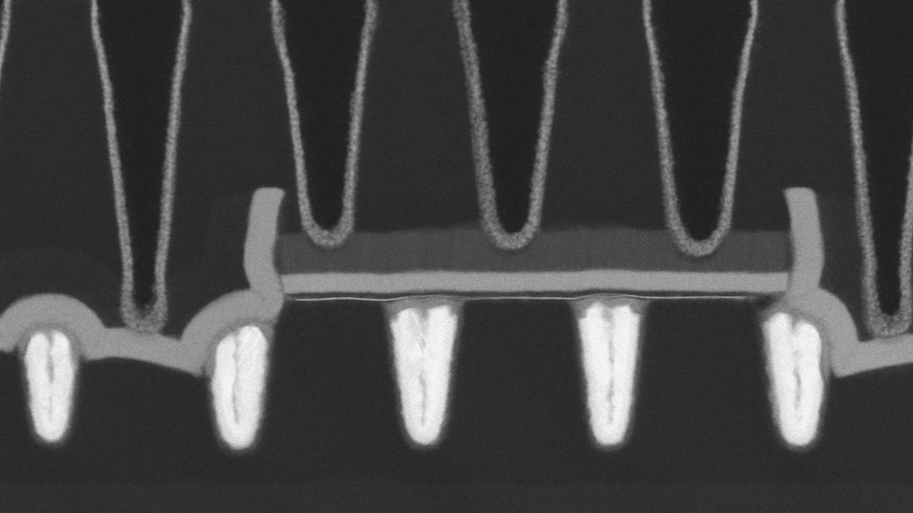
IMEC, a world-leading research and innovation hub in nanoelectronics and digital technologies based in Belgium, in close partnership with ASML and TSMC, has successfully developed and demonstrated a robust and scalable 300mm integrated process for both n-type and p-type field-effect transistors (FETs) that utilize 2D materials as their channel. This breakthrough, presented at the 2026 IEEE/JSAP VLSI Technology and Circuits Symposium, marks the first reported functional demonstration of n-type FETs employing molybdenum disulfide (MoS2) and p-type FETs utilizing tungsten disulfide (WS2) or tungsten diselenide (WSe2) at a challenging 50nm contact poly pitch (CPP), all while exhibiting desirable current-voltage (I-V) characteristics.
Technical Details
This innovative process represents a seamless integration of 2D material technology into existing 300mm silicon wafer fabrication lines. Specifically, molybdenum disulfide (MoS2) is employed as the channel material for the n-type FETs, while tungsten disulfide (WS2) or tungsten diselenide (WSe2) fulfills this role for the p-type FETs. The inherent atomic-scale thickness and high carrier mobility of these 2D materials are crucial enablers for realizing transistors scaled to unprecedented dimensions. The successful demonstration at a 50nm contact poly pitch (CPP) is a critically important metric, underscoring its relevance for the design of future ultra-compact Large-Scale Integration (LSI) circuits. This advancement strongly indicates the promise of 2D materials as viable next-generation semiconductor materials capable of surpassing the performance limits of conventional silicon.
Strategic Significance & Outlook
The successful demonstration of 2D material transistors on 300mm wafers represents a groundbreaking step that significantly accelerates the transition of this technology from ‘lab to fab.’ This development brings the realization of ultra-low-power, high-performance logic devices and memory based on 2D materials much closer to reality. Looking ahead, this technology is poised to dramatically enhance the performance and energy efficiency of a wide range of electronic products, including advanced smartphones, AI accelerators, and Internet of Things (IoT) devices. Moreover, this innovation is expected to stimulate further advancements in semiconductor manufacturing processes, thereby creating new business opportunities for related equipment and material industries. Continued research and development, coupled with successful commercialization efforts, for 2D material-based transistors are eagerly anticipated as they stand to become foundational technologies for next-generation computing paradigms.
Get our weekly technology intelligence — free
Receive an infographic that lets you judge at a glance whether each field’s analysis report is worth reading.
Subscribe Free — Weekly Tech Intelligence
By subscribing, you’ll receive Troy-Technical’s weekly technology intelligence newsletter.
- Your email and selected fields are used only to deliver the newsletter.
- We never share your information with third parties.
- You can unsubscribe anytime via the link in each email.
See our Privacy Policy for details.
Takes about a minute · Unsubscribe anytime

Comments