
Key Findings
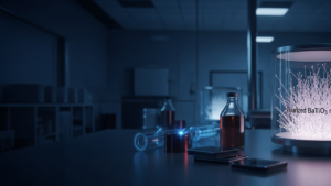
A seminal study published in Nature Nanotechnology reports a significant advancement in materials science: the successful growth of coherent 2D–3D van der Waals perovskite epitaxial heterostructures. Utilizing a novel cross-dimensional epitaxy technique, researchers created materials featuring atomically sharp interfaces, precisely controllable domains, and unique spiral chiroptical structures. Crucially, these heterostructures demonstrate stable, gate-tunable rectification properties, positioning them as a foundational material for highly advanced electronic and sensor technologies, including future biosensors.
Technical & Clinical Details
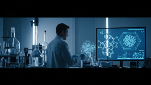
The essence of this breakthrough lies in the innovative method of joining 2D and 3D perovskite components, a technique dubbed ‘cross-dimensional epitaxy.’ This approach overcomes the long-standing challenges of lattice mismatch and interfacial defects that plague traditional heterostructure fabrication. The result is an exceptionally clean interface at the atomic level, which facilitates highly efficient charge carrier transport. This atomic-scale precision underpins the observed stable and gate-tunable rectification, a property vital for active electronic components. Furthermore, the discovery of spiral chiroptical structures suggests potential applications in highly selective sensing, where specific molecular chirality or polarization can be detected with unprecedented sensitivity, paving the way for next-generation biosensors capable of identifying minute quantities of target analytes.
Background & Context
Perovskite materials have garnered significant attention across photovoltaics, LEDs, and sensors due to their remarkable optoelectronic properties. However, stability issues and the complexity of integrating materials of different dimensions have hindered their widespread practical adoption. This research, by leveraging van der Waals interactions, effectively addresses these challenges, significantly expanding the potential of perovskite-based technologies. In an era demanding increasingly sensitive and stable sensor materials for diagnostics, environmental monitoring, and industrial control, this breakthrough is poised to have a profound impact across multiple application sectors.
Strategic Significance & Outlook
The newly developed 2D–3D van der Waals perovskite heterostructures are expected to find diverse applications in photonic devices, spintronics, and particularly in high-performance biosensors. Their gate-tunable characteristics open avenues for ‘smart sensors’ that can perform multiple functions within a single device. Future research will focus on assessing the long-term stability of these materials and developing scalable manufacturing processes. This technology represents a crucial step forward in foundational materials science, holding immense promise for the evolution of future electronic devices and advanced biosensing platforms globally.
Source: #
Get our weekly technology intelligence — free
Receive an infographic that lets you judge at a glance whether each field’s analysis report is worth reading.
Subscribe Free — Weekly Tech Intelligence
By subscribing, you’ll receive Troy-Technical’s weekly technology intelligence newsletter.
- Your email and selected fields are used only to deliver the newsletter.
- We never share your information with third parties.
- You can unsubscribe anytime via the link in each email.
See our Privacy Policy for details.
Takes about a minute · Unsubscribe anytime


Comments