Background
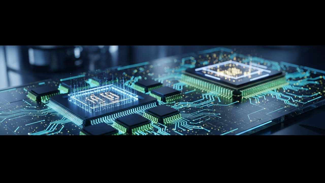
With the deceleration of Moore’s Law and the escalating demands of data-intensive applications like AI and High-Performance Computing (HPC), the semiconductor industry is actively seeking new scaling strategies. Chiplets, an approach where multiple smaller functional blocks are manufactured independently and then integrated into a single package using advanced packaging technologies, are widely recognized as one of the most promising solutions to this challenge. This strategy is already actively adopted by major players such as Intel (e.g., Meteor Lake with Foveros), AMD (e.g., Ryzen/EPYC with Zen chiplets), and NVIDIA (e.g., Hopper/Blackwell via CoWoS for GPU-HBM integration). However, the shift to chiplet designs entails new challenges in design, testing, and packaging, necessitating ecosystem-wide collaboration. Research institutions like Imec play a vital role in supporting the industry by providing foundational technologies and insights to facilitate this transition.
Key Findings
Imec has published an article analyzing the juncture at which it becomes economically and technically sensible to transition from monolithic Application-Specific Integrated Circuits (ASICs) to chiplet-based designs, particularly for AI, HPC, and data center applications. The analysis highlights that as silicon area approaches reticle size limits, advanced packaging technologies, coupled with improved interposer materials and finer bump pitches, are key to enabling high bandwidth and low energy transmission for chiplet integration.
Imec’s article examines the thresholds that make this transition a rational decision, primarily through the following technical factors:
- Silicon Area Limits: As large monolithic ASICs approach the reticle size limit of photomasks (approximately 26mm x 33mm), manufacturing yields decrease sharply, making production costs prohibitive.
- Interposer Technology: High-performance interconnect platforms, such as silicon or organic interposers, are necessary for efficient connection of multiple chiplets. Improved materials contribute to reduced signal loss and enhanced thermal management.
- Fine Bump Pitch: To increase the connection density between chiplets, fine bump pitch technologies, such as microbumps or hybrid bonding, are essential. This enables high-bandwidth and low-energy data transmission.
- System-Level Optimization: Chiplets allow for the combination of IP blocks manufactured at their respective optimal process nodes, improving overall system performance while controlling costs.
These technical advancements establish the practicality and advantages of chiplet designs.
Chiplet-based designs are expected to become mainstream in AI and HPC systems within the next few years. Imec’s research reinforces the technical and economic rationale for this trend, offering guidance for the industry to build next-generation systems more efficiently and innovatively. Continuous advancements in advanced packaging and substrate technologies will maximize the potential of chiplets, supporting the further evolution of AI technology and the expansion of its application domains. This is expected to accelerate a paradigm shift in semiconductor design and foster the emergence of new computing architectures.
Get our weekly technology intelligence — free
Receive an infographic that lets you judge at a glance whether each field’s analysis report is worth reading.
Subscribe Free — Weekly Tech Intelligence
By subscribing, you’ll receive Troy-Technical’s weekly technology intelligence newsletter.
- Your email and selected fields are used only to deliver the newsletter.
- We never share your information with third parties.
- You can unsubscribe anytime via the link in each email.
See our Privacy Policy for details.
Takes about a minute · Unsubscribe anytime


Comments