Key Findings
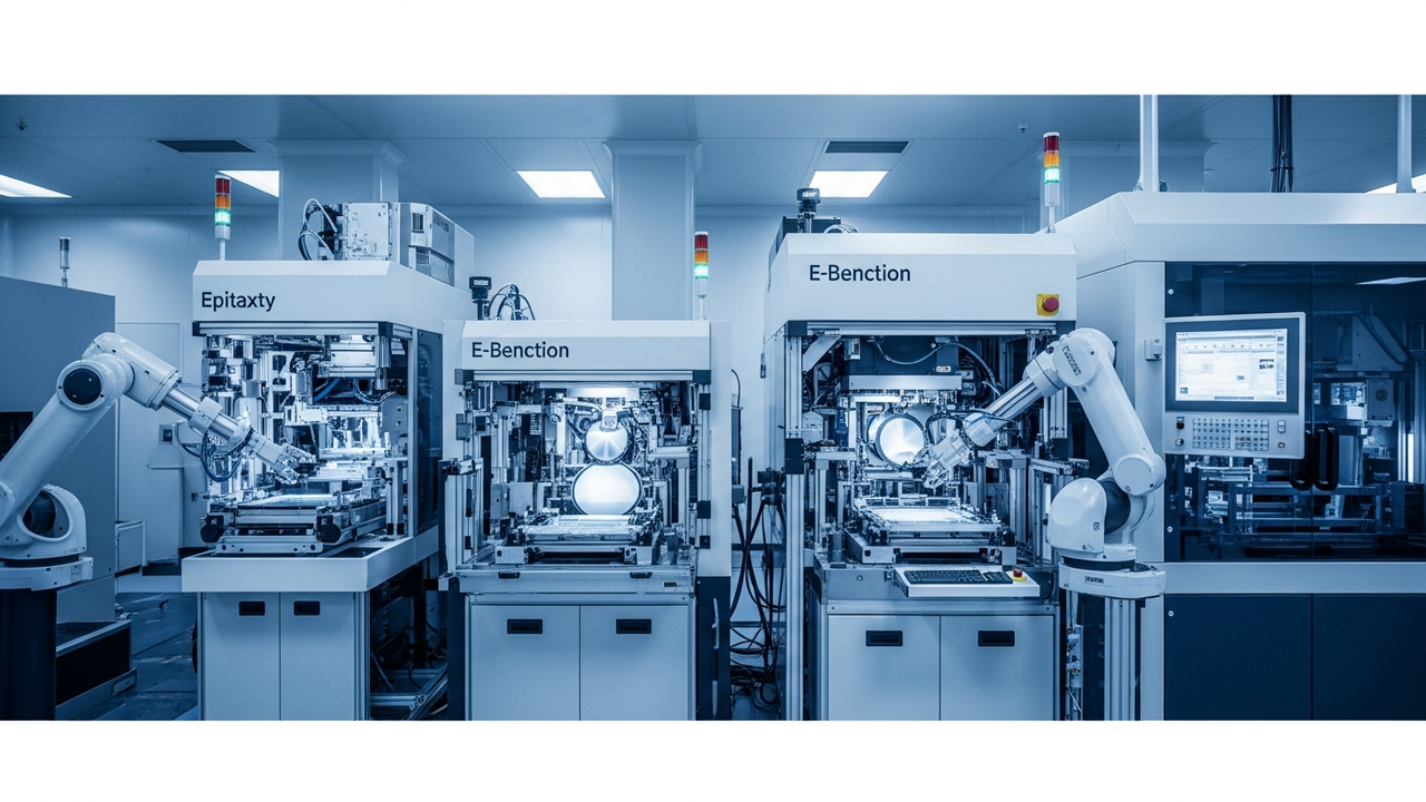
Applied Materials has unveiled a comprehensive suite of new chip manufacturing systems aimed at accelerating the construction of cutting-edge 3D chip architectures essential for powering next-generation AI applications. This robust portfolio includes advanced epitaxy systems optimized for DRAM production, alongside Chemical Mechanical Planarization (CMP), deposition, and innovative e-beam inspection systems specifically designed to enhance quality and yield in advanced packaging processes. A standout innovation is the SEMVision™ G7AP, which offers high-resolution defect review and automated classification across silicon, organic, and glass substrates, promising to dramatically expedite the yield learning process in advanced packaging.
Technical / Clinical Details
The new systems introduced by Applied Materials are engineered to address critical bottlenecks in semiconductor manufacturing and meet the complex requirements of AI chips:
- Epitaxy Systems for DRAM: DRAM, crucial for high-speed, high-capacity HBM (High Bandwidth Memory), demands intricate structures and precise film thickness control. The new epitaxy systems optimize DRAM performance and yield by meeting these stringent requirements, vital for maximizing the memory bandwidth of AI chips.
- CMP Systems for Advanced Packaging: In chiplet and 3D stacking technologies, ultra-high surface planarity of wafers is indispensable for accurate die bonding. The new CMP systems enhance material removal uniformity and surface quality, enabling next-generation packaging technologies like hybrid bonding.
- Deposition Systems: High-quality, uniform thin film formation is critical for insulation and interconnects between layers in advanced packaging. Applied Materials’ new deposition technologies meet these demands, ensuring signal integrity and reliable interconnectivity.
- SEMVision™ G7AP E-beam Inspection System: In advanced packaging, even microscopic defects on wafers and substrates can significantly impact the reliability of the final product. The SEMVision™ G7AP leverages high-resolution e-beam technology to rapidly and accurately detect and classify defects across a wide range of substrates, including silicon, organic (RDL), and glass. This capability enables early identification of root causes for defects, allowing for rapid optimization of manufacturing processes and dramatically shortening the yield learning cycle for AI chip production.
Background & Context
The increasing complexity and scale of AI models are revolutionizing semiconductor chip architectures. Facing the physical limits of traditional 2D scaling, the industry is shifting towards advanced packaging technologies such as 3D stacking, chiplets, and heterogeneous integration. These technologies are essential for improving data transfer rates, enhancing power efficiency, and achieving high performance within limited space. Leading semiconductor manufacturing equipment companies like Applied Materials play a central role in enabling this technological shift. The announcement of these new systems by Applied Materials clearly signifies an acceleration of innovation in AI-era semiconductor manufacturing.
Strategic Significance & Outlook
The new systems for DRAM and advanced packaging introduced by Applied Materials are critically important for resolving bottlenecks in AI chip manufacturing and accelerating the commercialization of next-generation AI technologies. Specifically, advanced inspection technologies like SEMVision™ G7AP are indispensable for improving yield and ensuring reliability in complex 3D packaging, contributing significantly to the mass production and cost efficiency of AI chips.
For researchers and engineers, these new tools provide the means to push the boundaries of DRAM design and explore more innovative packaging architectures. For investors, it is a strong signal that the growth of the AI market directly benefits the semiconductor manufacturing equipment sector, with technology leaders like Applied Materials poised for sustained growth. These technological innovations are set to enhance the performance and cost-efficiency of AI chips, further accelerating the adoption and integration of AI technology into society.
Get our weekly technology intelligence — free
Receive an infographic that lets you judge at a glance whether each field’s analysis report is worth reading.
Subscribe Free — Weekly Tech Intelligence
By subscribing, you’ll receive Troy-Technical’s weekly technology intelligence newsletter.
- Your email and selected fields are used only to deliver the newsletter.
- We never share your information with third parties.
- You can unsubscribe anytime via the link in each email.
See our Privacy Policy for details.
Takes about a minute · Unsubscribe anytime


Comments