Key Findings
IBM has introduced a sub-1-nanometer “NanoStack” semiconductor technology, promising a significant leap in performance for AI workloads. This innovative architecture aims to achieve up to a 50% performance increase or a remarkable 70% reduction in energy consumption compared to its predecessor, the 2nm technology.
Technical Details
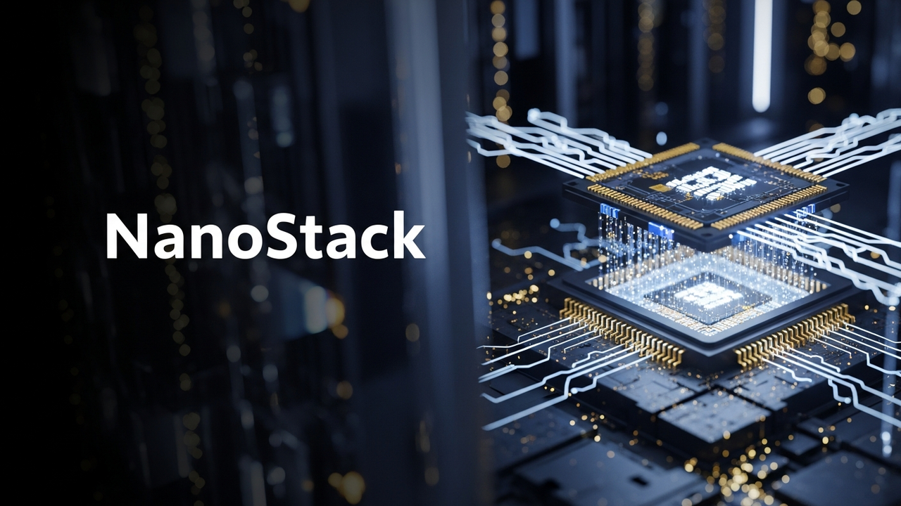
The NanoStack technology utilizes sequential 3D integration to vertically stack transistor structures. This method dramatically increases transistor density per unit area, allowing for more complex and compact circuitry within the chip. Furthermore, it provides the flexibility to combine different materials within individual stacked layers, enabling novel functionalities and optimizations that were previously challenging with traditional planar designs. This 3D stacking approach is critical for addressing the immense computational demands and memory bandwidth bottlenecks of advanced AI models, serving as a foundational technology for next-generation AI processors.
Background and Industry Context
The semiconductor industry is approaching the physical limits of Moore’s Law, making it increasingly difficult to achieve performance gains solely through transistor miniaturization. The rapid advancement of AI specifically demands ever-increasing computational resources and chips with higher performance and lower power consumption. IBM’s NanoStack tackles this challenge through a 3D integration approach, diverging from the conventional miniaturization path. Leading chip manufacturers like NVIDIA, Intel, and TSMC are also actively pursuing various forms of 3D integration, indicating that this technology will intensify competition across the semiconductor industry for AI-optimized chips.
Strategic Significance and Outlook
While still a research-phase device, the NanoStack technology holds immense potential to revolutionize AI accelerators, High-Performance Computing (HPC), and data center infrastructure. Its practical implementation could enable real-time processing of more complex AI models, extend battery life for edge AI devices, and reduce operational costs for data centers, thereby expanding the applicability of AI across numerous sectors. IBM aims to leverage this technology to maintain its leadership in future computing capabilities.
Get our weekly technology intelligence — free
Receive an infographic that lets you judge at a glance whether each field’s analysis report is worth reading.
Subscribe Free — Weekly Tech Intelligence
By subscribing, you’ll receive Troy-Technical’s weekly technology intelligence newsletter.
- Your email and selected fields are used only to deliver the newsletter.
- We never share your information with third parties.
- You can unsubscribe anytime via the link in each email.
See our Privacy Policy for details.
Takes about a minute · Unsubscribe anytime