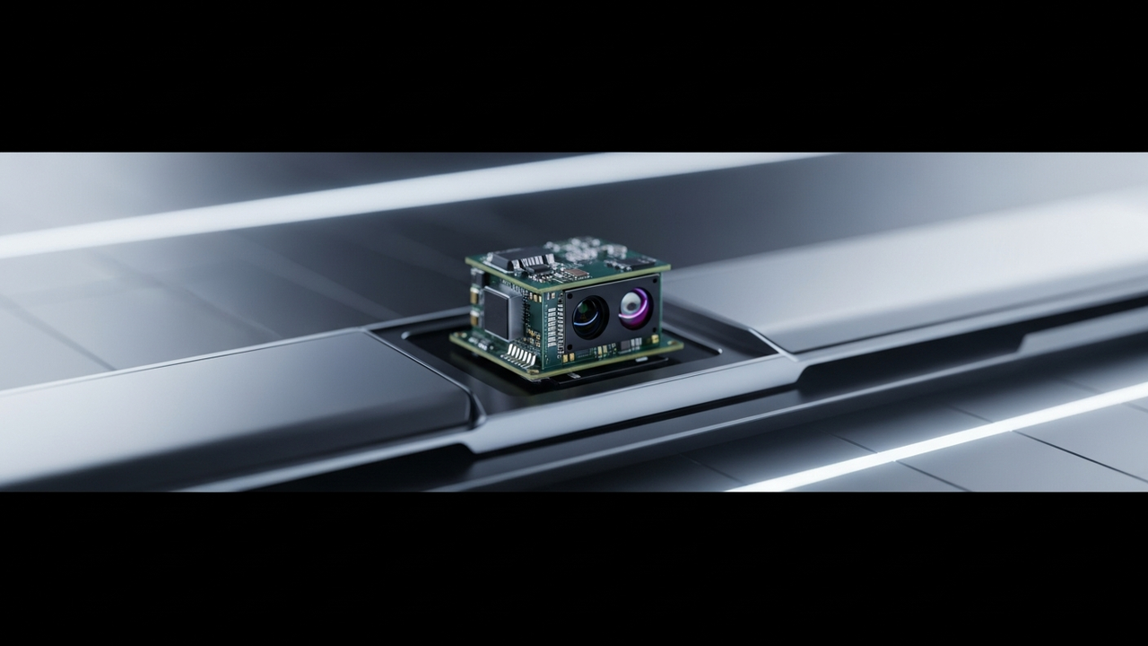
Background: The Quest for Compact, Robust LiDAR
LiDAR (Light Detection and Ranging) systems are pivotal for autonomous navigation, robotics, and advanced 3D mapping. However, conventional LiDAR often relies on bulky mechanical scanning mechanisms, which are expensive, fragile, and limited in form factor. Optical Phased Arrays (OPAs) offer a promising solid-state alternative, steering light electronically without moving parts. Yet, a persistent challenge in OPA technology has been the trade-off between achieving a wide field of view and maintaining high signal-to-noise ratio due to optical crosstalk between array elements.
Key Findings: MIT’s Crosstalk-Minimizing OPA on Silicon Photonics
Researchers at MIT have engineered a breakthrough silicon-photonics chip design for OPAs that fundamentally addresses the crosstalk problem, enabling a new generation of high-performance, compact LiDAR sensors. Key aspects of this innovation include:
- Novel Light-Emitting Structure: The new design incorporates microscopic curved structures that efficiently beam light from the chip into free space. This innovative approach significantly improves the efficiency of light coupling out of the silicon photonic chip, a long-standing hurdle for integrated optics.
- Crosstalk Suppression: Crucially, the design minimizes unwanted optical crosstalk between adjacent emitters in the array. This is achieved through careful waveguiding and optical isolation techniques, allowing for a much cleaner beam and higher fidelity 3D sensing. By suppressing crosstalk, the OPA can scan a wider field of view without introducing debilitating noise.
- Solid-State Advantages: Being entirely solid-state, the new OPA chip eliminates the need for any mechanical moving parts. This intrinsically enhances durability, reduces manufacturing complexity, and allows for miniaturization, making the LiDAR sensor immune to vibrations and environmental factors that affect traditional systems.
- Wider Field of View with Low Noise: The combination of efficient light extraction and crosstalk suppression allows the OPA to achieve a wider scanning angle without compromising on signal integrity, a crucial feature for comprehensive environmental perception in applications like autonomous vehicles.
Technical Significance & Outlook: Redefining 3D Sensing
This MIT advancement holds profound implications for the future of LiDAR and broader 3D sensing technologies. The ability to create compact, durable, and high-performance solid-state LiDAR chips addresses key barriers to widespread adoption in cost-sensitive and mission-critical applications. By making LiDAR smaller, more reliable, and energy-efficient, this technology will:
- Accelerate Autonomous Vehicle Development: Enable the integration of multiple, redundant LiDAR sensors into vehicles without aesthetic or cost penalties, improving safety and perception capabilities.
- Advance Aerial Surveying and Robotics: Provide robust and precise 3D mapping solutions for drones and industrial robots operating in challenging environments.
- Revolutionize AR/VR Devices: Facilitate the development of compact augmented reality and virtual reality systems with enhanced spatial awareness.
Ultimately, this research pushes us closer to ‘operational 3D sensing,’ where continuous, embedded spatial measurement becomes ubiquitous in everyday systems, transforming how we interact with and navigate our physical world. The precise control over light at the chip scale achieved here marks a significant step towards realizing truly miniature and performant optical sensing systems.
Source: https://www.photonics.com/Articles/New-Optical-Phased-Array-Design-Could-Slim-Down/a72254








Comments