Background
The relentless pursuit of miniaturization in the semiconductor industry has pushed conventional photolithography to its physical and economic limits. As feature sizes approach the sub-10 nanometer regime, the complexities and costs associated with optical lithography, including advanced light sources and intricate mask designs, become prohibitive. This scenario has spurred significant research and development into alternative nanofabrication techniques capable of delivering higher resolution, greater throughput, and lower cost per feature.
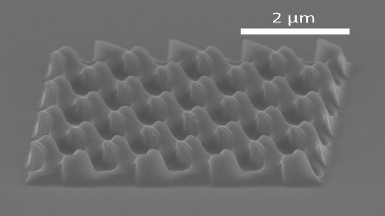
Key Findings / Results
Nanoimprint Lithography (NIL) stands out as a promising next-generation nanofabrication method. Unlike photolithography, NIL employs a direct mechanical embossing process where a rigid master mold (stamp) physically deforms a resist layer on a substrate. This physical transfer bypasses optical diffraction limits, allowing for pattern replication with resolutions well below 10 nm, matching the capabilities of electron beam lithography but at potentially much higher throughput. Key characteristics include:
- High Resolution: Capable of replicating features down to sub-10 nm with high fidelity, driven by the physical dimensions of the master mold.
- Cost-Effectiveness: Eliminates expensive optical systems and complex multi-exposure processes, leading to potentially lower fabrication costs per wafer.
- Scalability and Throughput: Enables parallel patterning over large areas, making it suitable for high-volume manufacturing environments.
- Versatility: Applicable to a wide range of materials and substrates, including polymers, metals, and semiconductors.
Recent advancements have focused on improving mold durability, defect control during the imprinting process, and achieving precise overlay alignment, which are crucial for multi-layer device integration. Companies like Canon (developing roll-to-roll NIL) and large semiconductor foundries are actively exploring NIL for critical layers in advanced node manufacturing.
Technical Significance & Outlook
The technical significance of NIL lies in its potential to enable the fabrication of devices that are currently challenging or uneconomical with existing technologies. For logic and memory devices, NIL could define critical dimensions for FinFETs, gate-all-around (GAA) nanowires, and high-density memory arrays. In data storage, it promises the creation of bit-patterned media for hard disk drives, significantly increasing storage density beyond 10 Tbit/inch². Beyond semiconductors, NIL’s applications extend to photonics (e.g., gratings, waveguides), bio-sensors (e.g., lab-on-a-chip devices), and advanced MEMS/NEMS. However, persistent challenges include the need for defect-free molds, robust resist materials, high-speed and accurate alignment systems, and reliable mold release mechanisms. Overcoming these hurdles will be paramount for NIL to transition from a specialized niche to a mainstream fabrication technology, potentially disrupting the semiconductor manufacturing landscape and enabling a new generation of high-performance, low-cost nanoscale devices.


Comments