May 2026– date –
-

Samsung Electro-Mechanics and Sumitomo Chemical Group Partner to Establish Glass Core Substrate Joint Venture
企業発表 South Korea Overview Samsung Electro-Mechanics and Sumitomo Chemical Group have signed an MOU to establish a joint venture for manufacturing "glass core" substrates, a critical material for next-generation advanced packaging. Ai... -
SK Hynix Validates 12-Die Hybrid Bonded HBM Stack Amidst Heated AI Memory Race
専門メディア South Korea Overview SK Hynix has successfully verified a 12-die HBM stack using hybrid bonding, demonstrating significant progress in its next-generation packaging technology for HBM4 and HBM5. While actively improving yiel... -
Samsung Electronics Pioneers HBM4 Mass Production with Hybrid Bonding, Solidifying Market Lead
専門メディア South Korea Overview Samsung Electronics is strategically deploying dedicated hybrid bonding lines in its domestic facilities for HBM4, aiming to secure market leadership. The company has successfully commenced mass producti... -
SK Hynix Initiates HBM Packaging Hub Construction in Cheongju to Bolster AI Memory Capacity
専門メディア South Korea Overview SK Hynix has broken ground on a substantial advanced packaging facility in Cheongju Technopolis, signaling a strategic shift in AI semiconductor competition from wafer fabrication to performance-critical... -
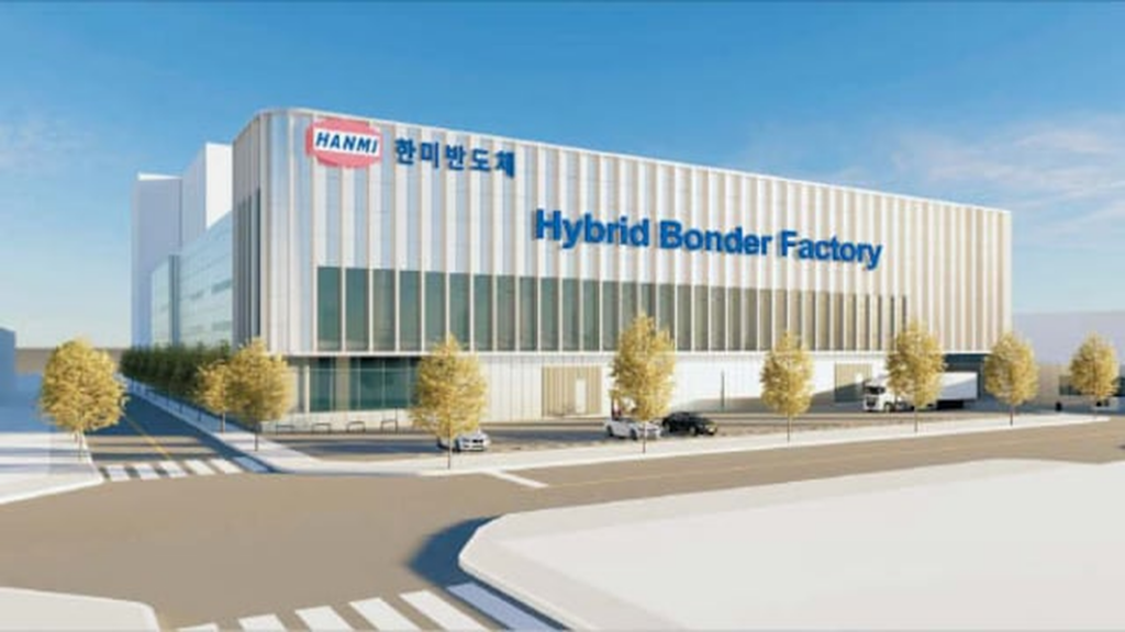
Hanmi Semiconductor Unveils Second-Gen Hybrid Bonder for Advanced HBM Stacking, Investing $67M in New Factory
専門メディア South Korea Overview Hanmi Semiconductor is set to introduce its second-generation hybrid bonder prototype this year, crucial for next-generation HBM mass production with over 20 stacked layers. Concurrently, the company is ... -
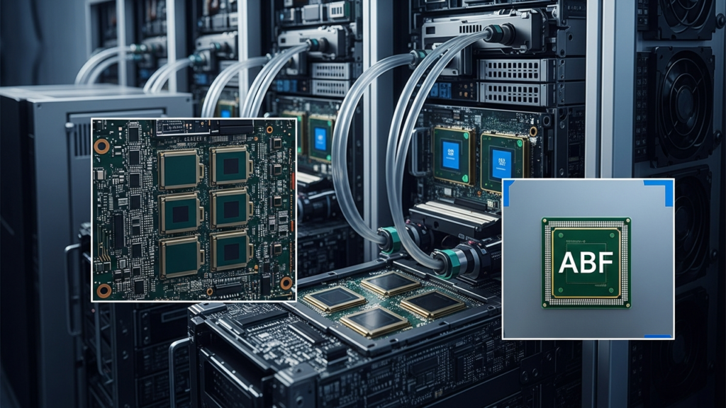
ABF Substrate Becomes Critical Bottleneck in AI Hardware Supply Chain, Driven by Ajinomoto’s Dominance
専門メディア (分析) Taiwan Overview Ajinomoto Build-up Film (ABF), an essential insulating dielectric for high-performance substrates, has emerged as an unexpected bottleneck in the AI hardware ecosystem due to Ajinomoto Fine-Techno's ne... -
TSMC Unveils SoIC 3D Stacking Roadmap: Achieving 4.5µm Pitch by 2029, Enabling Face-to-Face Chiplet Integration for Fujitsu Monaka CPU
専門メディア Taiwan Overview TSMC has revealed its SoIC (System on Integrated Chips) 3D stacking roadmap, targeting a 4.5-micron pitch by 2029, down from today's 6 microns. This advanced face-to-face (F2F) chiplet stacking technology, pa... -
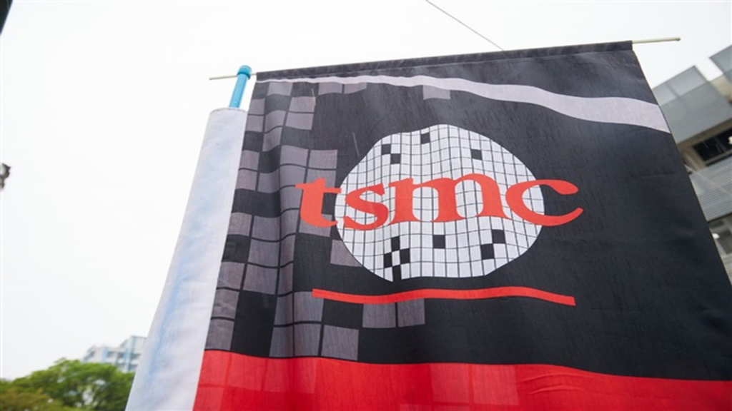
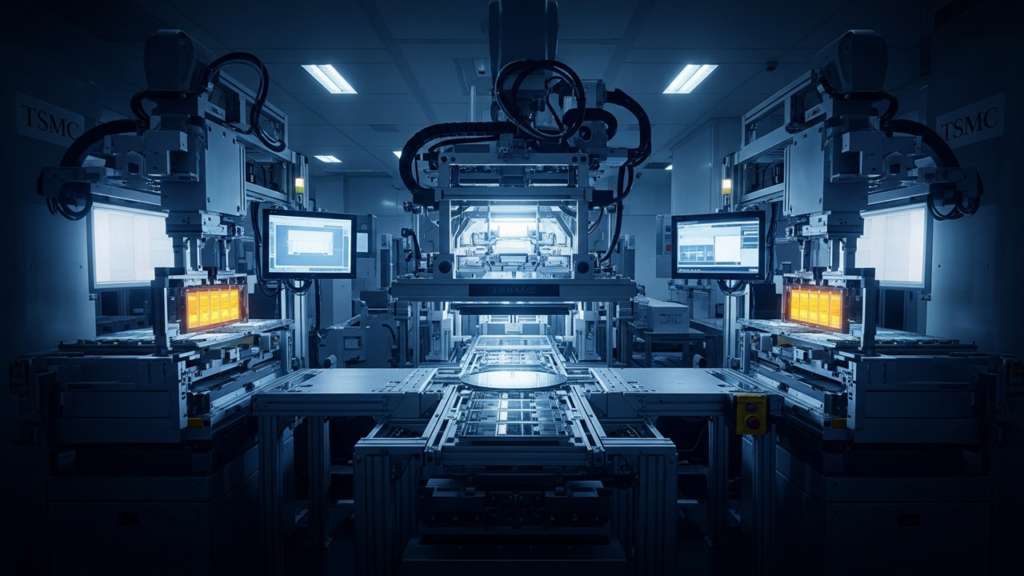
TSMC Forges Exclusive CoPoS Supply Chain to Secure Next-Gen AI Packaging Dominance
専門メディア Taiwan Overview TSMC is reportedly implementing a highly exclusive supply chain strategy for CoPoS, its next-generation panel-level packaging technology, to solidify its leadership in AI semiconductors. This move, involving ... -
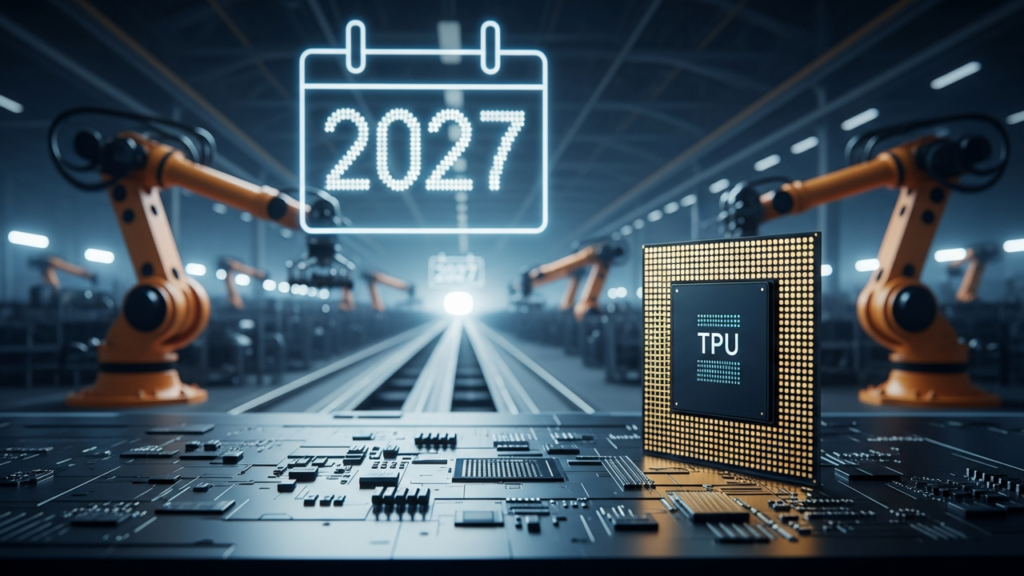
TSMC’s CoWoS Bottleneck Threatens to Delay Google TPU Mass Production to 2027
専門メディア Taiwan Overview Chronic shortages in TSMC's CoWoS advanced packaging capacity are projected to delay mass production of Google's custom AI chips (TPU) until 2027. Despite TSMC's aggressive expansion plans targeting 120,000 w... -
TSMC Accelerates Advanced Packaging Capacity Expansion to Meet Exploding AI Demand
専門メディア Taiwan Overview TSMC is rapidly scaling its advanced CoWoS and SoIC packaging capacity to address the surging demand for AI chips. With 18 new fabs and advanced packaging facilities under construction globally, this expansio...