Background
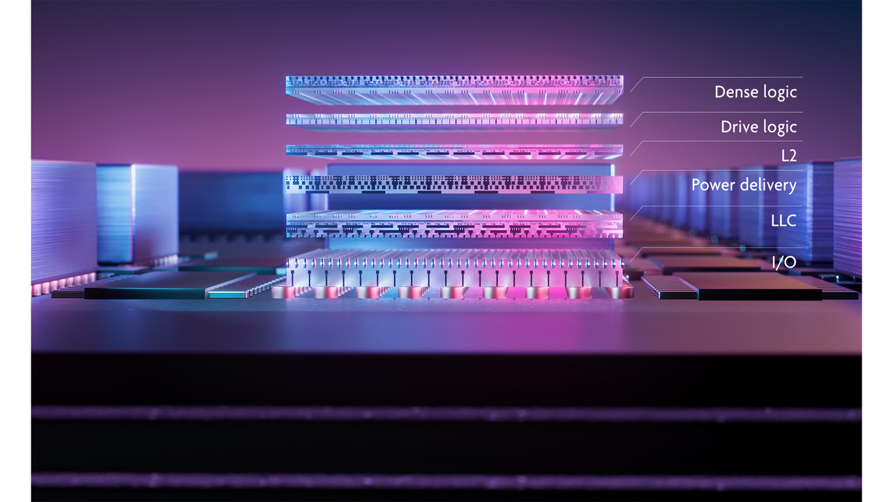
As conventional CMOS scaling approaches its fundamental physical limits, three-dimensional (3D) integration has emerged as a critical pathway to continue enhancing semiconductor performance and functionality. This approach is particularly vital for demanding applications such as AI accelerators and advanced chiplet platforms, which necessitate ultra-high-density interconnects and significantly increased bandwidth. However, a persistent challenge in vertically stacking chips has been ensuring precise alignment accuracy and robust connection reliability between tiers. Imec and EV Group’s latest achievement provides a decisive solution to this long-standing hurdle, accelerating the realization of future systems—including AI, High-Performance Computing (HPC), and advanced smart vision systems—that require the extremely high interconnect densities envisioned by the CMOS 2.0 scaling paradigm.
Key Findings
Imec, a world-leading semiconductor research institute, in collaboration with EV Group (EVG), a prominent supplier of wafer processing equipment, recently showcased a robust, high-yield wafer-to-wafer hybrid bonding technology at the 2026 IEEE Electronic Components and Technology Conference (ECTC). This groundbreaking demonstration featured a 200-nanometer (nm) copper interconnect pad pitch, achieving a new world-record accuracy: a post-bond overlay vector of less than 40 nm across a full 300mm wafer. This precision represents a significant leap forward, critically enabling the realization of next-generation 3D integrated circuits (ICs).
Technical Details
The demonstrated hybrid bonding technology masterfully integrates both metal-to-metal (primarily copper-to-copper, or Cu-Cu) and dielectric-to-dielectric (oxide-to-oxide) bonding processes within a single interface. This innovative approach ensures both electrical continuity and robust mechanical integrity without the need for traditional solder or microbumps. The research utilized a sophisticated test vehicle incorporating routable interconnects, specifically designed to demonstrate the feasibility of high-density logic-on-logic and memory-on-logic tier stacking. The exceptional overlay accuracy and impressive yield were critically achieved through two key optimizations: the specific use of silicon carbon nitride (SiCN) as the dielectric material, and the meticulous optimization of the chemical mechanical polishing (CMP) step performed immediately prior to bonding. This combined technique facilitates simultaneous Cu-to-Cu and oxide-to-oxide bonding at aggressive sub-micron pitches, dramatically enabling finer interconnects and substantially reducing parasitic capacitance and inductance compared to conventional packaging methods.
Strategic Significance and Outlook
The realization of this record-breaking hybrid bonding technology marks a profound advancement in the evolution of 3D IC stacking, unlocking new paradigms for the design of high-performance AI accelerators and other advanced chiplet-based system architectures. By dramatically reducing interconnect path lengths, this technology promises significantly improved data transfer speeds and substantial reductions in power consumption. This capability has the potential to revolutionize the performance and energy efficiency of next-generation AI hardware and High-Performance Computing (HPC) systems. The ongoing collaboration between Imec and EVG is poised to continue pushing the technical boundaries of fine-pitch interconnection, thereby fostering widespread innovation across the entire semiconductor industry.


Comments