Key Findings
This review comprehensively discusses the transformative potential of metasurfaces, fabricated using advanced semiconductor manufacturing techniques, for neutral-atom trapping. It highlights how these engineered optical components can enable the construction of scalable optical-tweezer arrays capable of trapping millions of neutral atoms, generate sophisticated trapping profiles such as optical bottle beams, and consolidate multiple functionalities into a single optical element. The core message is that metasurfaces can drastically reduce the number of discrete optical components, thereby simplifying the packaging and deployment of compact and portable quantum systems.
Technical / Clinical Details
- Metasurfaces Defined: Metasurfaces are two-dimensional arrays of nanoscale structures engineered to control light’s phase, amplitude, and polarization with unprecedented precision. They offer ultra-thin and multi-functional optical components, surpassing the capabilities of conventional bulk optics.
- Application to Neutral-Atom Trapping: Neutral atoms serve as a leading platform for quantum computing, high-precision sensors, and atomic clocks. Metasurfaces precisely sculpt laser light to create intricate optical traps, enabling the spatial confinement, cooling, and manipulation of these atoms.
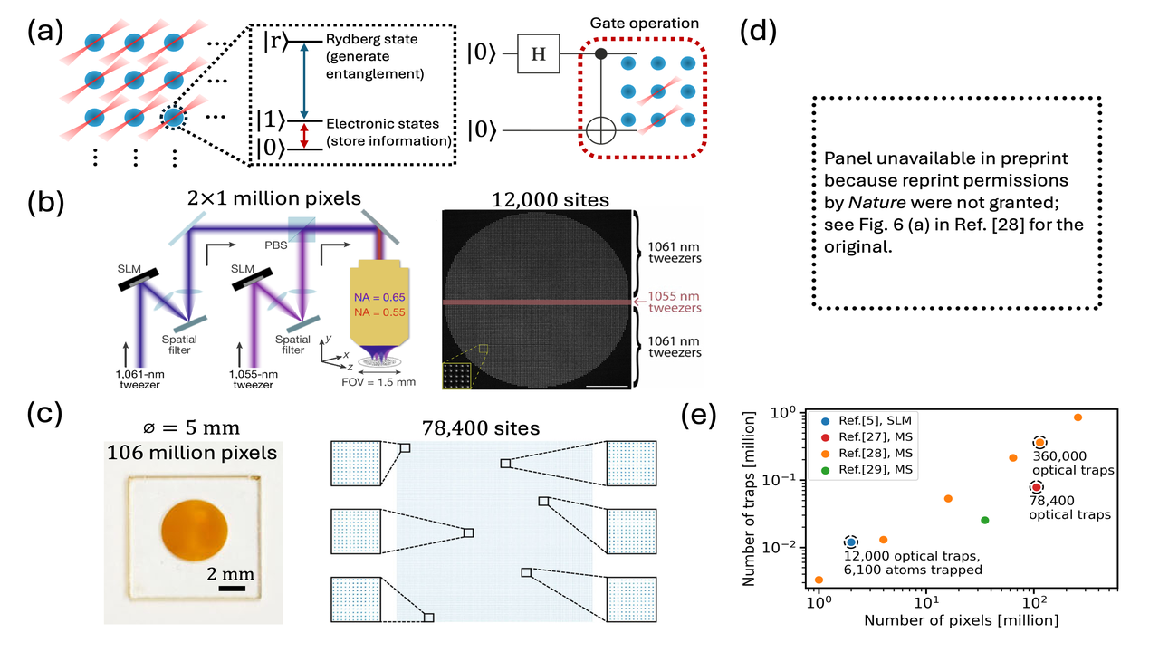
- Scalable Optical Tweezer Arrays: Traditional optical tweezer arrays for atom trapping are complex, requiring numerous discrete optical elements and precise alignment, which hinders scalability. Metasurfaces, being mass-producible using lithographic techniques, can create millions of trapping sites on a single chip, offering a pathway to dramatically increase the number of qubits for quantum computers.
- Complex Trapping Profiles: Metasurfaces can generate sophisticated light fields, such as optical bottle beams (light traps with a dark core), which are crucial for extending atomic coherence times and improving the fidelity of quantum operations.
- Multi-Functionality: The ability to integrate multiple optical functions—trapping, cooling, manipulating, and detecting atoms—onto a single metasurface simplifies quantum system architecture, reduces size, and enhances robustness.
Background & Context
Quantum technologies, promising revolutions in computing, communication, and sensing, face significant challenges in miniaturization, stability, and scalability. For neutral-atom-based quantum systems, precise control and large-scale integration of atoms are paramount. Metasurface technology emerges as a highly promising solution to address these challenges, offering a path to build more compact, robust, and deployable quantum devices.
Strategic Significance & Outlook
Metasurface technology is a key enabler for realizing compact and portable quantum systems. The review points out critical practical challenges in metasurface design (e.g., material choice, broadband operation, thermal management) and the importance of seamless integration into complex optical and vacuum systems. Successfully addressing these challenges will allow metasurfaces to have a profound impact on:
- Quantum Computing: Facilitating the development of quantum processors with millions of qubits.
- High-Precision Atomic Clocks: Enabling compact and robust next-generation atomic clocks.
- Ultra-Sensitive Quantum Sensors: Expanding applications in magnetometry, medical imaging, and gravitational wave detection.
This technology is poised to accelerate the commercialization of quantum technologies, forming an indispensable foundation for the future information society. The ability to dramatically reduce the size and complexity of atomic quantum systems will democratize access to these powerful technologies and open up entirely new markets.


Comments