Key Findings
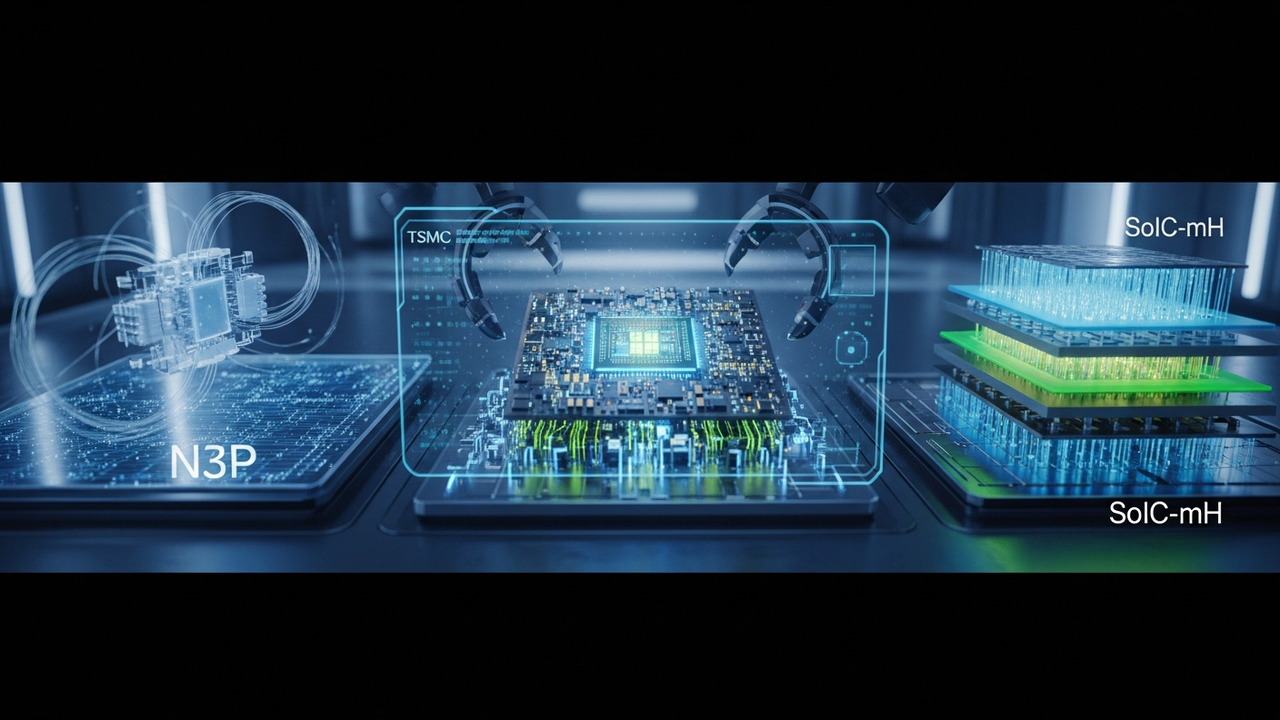
Apple’s next-generation M5 Ultra chip is reportedly set to achieve unprecedented performance and efficiency by combining TSMC’s N3P process technology with the innovative advanced packaging technique, SoIC-mH (System-on-Integrated-Chips – molded horizontal packaging). This technological integration, expected to debut in Mac Studio products unveiled at WWDC, will establish a new benchmark for high-density heterogeneous integration.
Technical Deep Dive
The adoption of TSMC’s N3P process (an enhanced version of the 3nm process) for the M5 Ultra chip will bring further advancements in transistor density and power efficiency. N3P offers higher performance and superior yield characteristics compared to N3E, making it an ideal choice for large-scale, high-performance chips. However, the true innovation of the M5 Ultra lies in its packaging technology.
SoIC-mH is a variation of TSMC’s advanced 3D stacking technology, SoIC, specifically optimized for high-density heterogeneous integration. Key features of SoIC-mH include:
- Molded Horizontal Packaging Architecture: Multiple chips are arranged horizontally and then encapsulated entirely within a molding material, optimizing both robustness and thermal management.
- Bump-less Hybrid Bonding: This technique directly bonds chips using copper-to-copper connections at the wafer level, bypassing conventional micro-bumps. This enables connection pitches finer than 10µm, drastically shortening signal transmission paths, and consequently achieving significant reductions in signal delay and improvements in power efficiency.
- High-Density Integration: Seamlessly integrates multiple logic dies and other functional chiplets at the wafer level, delivering levels of integration and functionality previously unattainable with conventional packaging.
These technological advancements will enable the M5 Ultra to accommodate more cores and eliminate inter-chip communication bottlenecks, leading to dramatic performance improvements in graphics processing, AI/ML workloads, and High-Performance Computing (HPC) tasks. This will significantly elevate the processing power of professional workstations like the Mac Studio.
Background and Industry Context
Since introducing its custom-designed M-series chips into Mac products, Apple has led the industry in performance and power efficiency. Chiplet architectures and advanced packaging have emerged as primary means to enhance chip performance, especially as Moore’s Law confronts its physical limits. TSMC’s SoIC is one of the industry’s most advanced packaging technologies, notably adopted in NVIDIA’s AI accelerators. Apple’s embrace of SoIC-mH for the M5 Ultra underscores its aggressive investment not only in chip manufacturing but also in packaging technology to extract peak performance. This move suggests a further convergence of chip design and packaging across the broader semiconductor industry.
Future Outlook
The adoption of TSMC’s N3P process and SoIC-mH in the Apple M5 Ultra will undoubtedly set new benchmarks for professional workstation performance. This high-density packaging technology is anticipated to extend to more Apple products in the future, particularly devices requiring significant AI and HPC capabilities. The M5 Ultra’s debut will not only bolster the competitiveness of Apple’s Mac products in the high-end market but also serve as a crucial example of how advanced packaging technologies like SoIC-mH will shape the future of heterogeneous integration and chiplet design. This is expected to pave the way for further innovation and performance enhancements across the semiconductor industry.


Comments