Key Findings
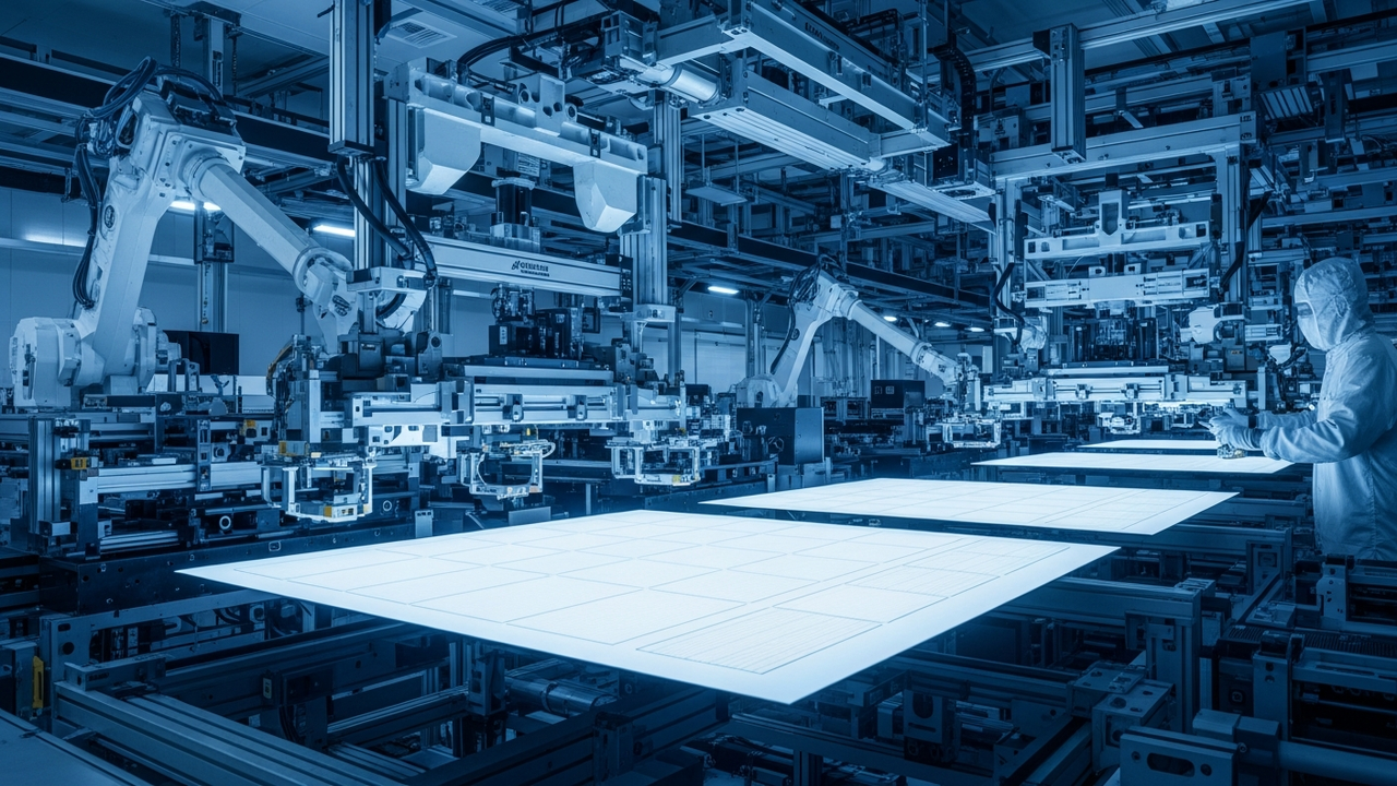
Asahi Kasei has introduced a groundbreaking photosensitive film for panel-level semiconductor packaging, integrating its proprietary PIMEL photosensitive polyimide (PSPI) and SUNFORT dry film photoresist technologies. This advancement is poised to revolutionize advanced packaging by enabling highly precise and uniform material application on large panels.
Technical / Clinical Details
The new film technology addresses critical challenges in applying insulating and patterning materials uniformly across large panel substrates, a prerequisite for next-generation semiconductor devices. It significantly simplifies the process of creating multiple insulating layers in complex designs and fabricating high-aspect-ratio copper pillars essential for 3D stacking architectures. By overcoming previous manufacturing limitations, this innovation is expected to enhance yield and streamline production workflows. The film is currently undergoing rigorous evaluation by customers, with promising results anticipated to accelerate its commercial adoption.
Background & Context
The semiconductor industry is witnessing a strategic shift from traditional front-end scaling to advanced back-end packaging, driven by the increasing demand for higher performance and integration in areas like AI and high-performance computing. As Moore’s Law faces physical limits, technologies that enable heterogeneous integration and 3D stacking have become paramount. Asahi Kasei’s new photosensitive film directly supports these trends, offering a solution to the thermal management and reliability issues inherent in dense, multi-layered chip designs, which are particularly critical for AI accelerators and other advanced processors.
Strategic Significance & Outlook
This development by Asahi Kasei holds significant implications for semiconductor manufacturing, promising not only improved performance but also potential cost reductions in advanced packaging. The ability to precisely control material application on large panels paves the way for more efficient mass production of complex chips. This positions Asahi Kasei as a key enabler for the ongoing evolution of AI, autonomous driving, and data center technologies, facilitating the creation of more powerful and reliable semiconductor components globally. The successful commercialization of this film will mark a crucial step towards the widespread adoption of panel-level packaging as a standard for high-performance devices.
Source: https://thepackhub.com/innovation/photosensitive-film-for-panel-level-semiconductor-packaging/
Get our weekly technology intelligence — free
Receive an infographic that lets you judge at a glance whether each field’s analysis report is worth reading.
Subscribe Free — Weekly Tech Intelligence
By subscribing, you’ll receive Troy-Technical’s weekly technology intelligence newsletter.
- Your email and selected fields are used only to deliver the newsletter.
- We never share your information with third parties.
- You can unsubscribe anytime via the link in each email.
See our Privacy Policy for details.
Takes about a minute · Unsubscribe anytime


Comments