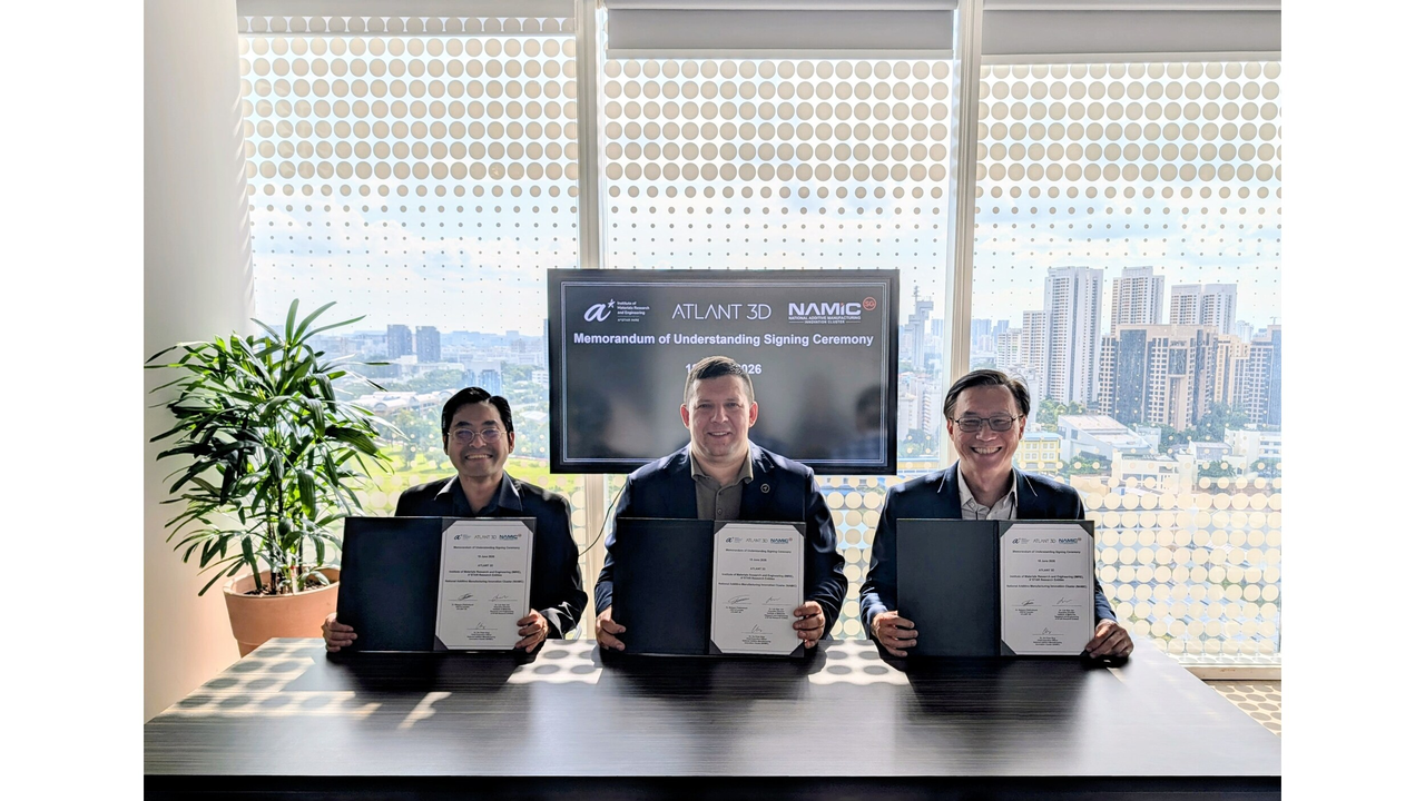
ATLANT 3D, A*STAR IMRE, and NAMIC Launch New AI-Driven Materials Discovery Hub in Singapore
ATLANT 3D, a leader in innovative 3D printing technology, has entered into a strategic Memorandum of Understanding (MOU) with Singapore’s A*STAR Institute of Materials Research and Engineering (A*STAR IMRE) and the National Additive Manufacturing Innovation Cluster (NAMIC). The objective of this partnership is to establish an ‘Advanced Materials Development Hub’ (A-HUB) in Singapore, dedicated to pioneering AI-driven materials discovery. This collaborative initiative is set to become a critical foundation for accelerating materials innovation in the rapidly evolving fields of semiconductors, photonics, and advanced packaging.
Integration of DALP® Technology with Singaporean Expertise
The A-HUB will integrate ATLANT 3D’s proprietary DALP® (Direct Atomic Layer Processing) technology with A*STAR IMRE’s world-class, deep expertise in materials engineering, and NAMIC’s robust additive manufacturing capabilities. DALP® technology enables precise material deposition at the atomic layer scale. By combining this with AI and machine learning, the process of discovering, synthesizing, and characterizing new materials can be dramatically accelerated. This synergy will facilitate the rapid exploration and optimization of high-performance materials, a feat often challenging with traditional material development methods.
Key Application Areas and Global Impact
The establishment of this advanced materials development hub will primarily focus on the following application areas:
- Advanced Packaging: Developing higher performance and more reliable material solutions for next-generation semiconductor packaging, addressing the needs of AI and high-performance computing.
- Silicon Photonics: Exploring innovative materials for silicon photonic devices, which are crucial for improving optical communication and data transfer speeds.
- Semiconductor Manufacturing: Developing new materials that contribute to yield improvement and cost reduction in semiconductor manufacturing processes, which are increasingly miniaturized and high-performing.
This partnership holds strategic significance for Singapore, solidifying its position as a vital hub for advanced materials research and development in the Asia-Pacific region. The A-HUB is expected to contribute to the global materials science community and serve as an open innovation platform for solving complex technological challenges faced by industries. In the long term, this initiative is anticipated to be a driving force behind material science breakthroughs essential for realizing sustainable, high-performance future electronics and devices.
Get our weekly technology intelligence — free
Receive an infographic that lets you judge at a glance whether each field’s analysis report is worth reading.
Subscribe Free — Weekly Tech Intelligence
By subscribing, you’ll receive Troy-Technical’s weekly technology intelligence newsletter.
- Your email and selected fields are used only to deliver the newsletter.
- We never share your information with third parties.
- You can unsubscribe anytime via the link in each email.
See our Privacy Policy for details.
Takes about a minute · Unsubscribe anytime


Comments