Key Findings
BE Semiconductor Industries (BESI) has substantially revised its long-term business outlook, elevating its annual revenue target from the previous range of €1.5-1.9 billion to €1.7-2.2 billion. Concurrently, the lower bound of its operating margin target has also been increased from 40% to 45%. This assertive revision stems from an unprecedented surge in demand, primarily driven by 2.5D packaging for AI applications, photonics integration in data centers, and emerging use cases for hybrid bonding in logic, memory, and Co-packaged optics (CPO). BESI firmly believes these advanced technologies are integral to the semiconductor industry’s next phase of growth.
Technical / Clinical Details
Hybrid bonding is a direct die-to-die or die-to-wafer interconnect technology that achieves significantly higher interconnect density and shorter electrical paths compared to conventional wire bonding or flip-chip bonding. This leads to dramatic improvements in data transfer speeds and reductions in power consumption. In the context of 2.5D/3D packaging for AI accelerators and High-Performance Computing (HPC), where multiple chiplets (e.g., logic and HBM) must be integrated with extreme precision, hybrid bonding has emerged as a key enabling technology.
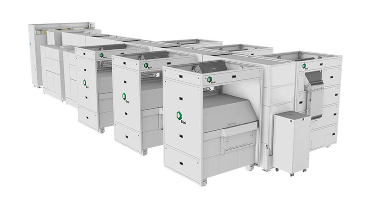
BESI is a leading equipment provider in hybrid bonding technology, with its bonders capable of joining dies with sub-micron level accuracy. This technology is driving demand in several critical areas:
- 2.5D AI-related Data Centers: Providing high-speed, high-density connections within GPU packages integrating AI chips and HBM memory.
- Photonics Applications: Essential for the performance enhancement of silicon photonics chips and their integration with optical I/O components.
- Advanced Logic and Memory Integration: Used for high-density inter-chiplet connections as chiplet architectures become more prevalent.
- Co-packaged Optics (CPO): Plays a vital role in integrating switching chips and optical transceivers within a single package, enabling ultra-fast data transmission and low power consumption.
These technologies directly contribute to meeting the increasing bandwidth demands and improving the power efficiency of data centers, accelerating the evolution of AI infrastructure.
Background & Context
Facing the slowdown of Moore’s Law, the semiconductor industry is increasingly focusing on performance enhancement through packaging innovation, rather than solely through transistor miniaturization. In this ‘More than Moore’ era, advanced packaging, especially hybrid bonding, is pivotal for the development of the chiplet ecosystem and the realization of heterogeneous integration. The rise of AI further accelerates this trend, as the exponential increase in data center power consumption and data traffic necessitates urgent improvements in semiconductor component integration density and efficiency.
Equipment manufacturers like BESI are at the forefront of this technological shift, with their innovative bonding solutions enabling the fabrication of next-generation semiconductors. BESI’s upward revision of its targets clearly indicates the maturation of the hybrid bonding market and the strong growth momentum it imparts to the semiconductor manufacturing equipment market.
Strategic Significance & Outlook
BESI’s elevated long-term revenue and operating margin targets validate the establishment of hybrid bonding technology as a sustainable growth engine for the semiconductor industry. As demand for AI, HPC, and data centers continues to accelerate, advanced packaging technologies like hybrid bonding will become even more indispensable. Consequently, BESI is highly likely to maintain high growth and profitability in the foreseeable future.
For researchers and engineers, hybrid bonding technology offers expanded opportunities for novel design freedom and performance improvements. Further miniaturization of chiplets and integration with optical devices will enable the creation of new applications previously unimaginable. For investors, BESI remains an attractive investment target as a company strategically positioned within the semiconductor supply chain, directly benefiting from the AI-driven economy. Hybrid bonding is set to strengthen its role not just as a manufacturing process, but as a foundational technology shaping next-generation semiconductor architectures.
Get our weekly technology intelligence — free
Receive an infographic that lets you judge at a glance whether each field’s analysis report is worth reading.
Subscribe Free — Weekly Tech Intelligence
By subscribing, you’ll receive Troy-Technical’s weekly technology intelligence newsletter.
- Your email and selected fields are used only to deliver the newsletter.
- We never share your information with third parties.
- You can unsubscribe anytime via the link in each email.
See our Privacy Policy for details.
Takes about a minute · Unsubscribe anytime


Comments