Key Findings
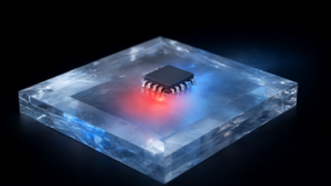
In a review of the IEEE ECTC (Electronic Components and Technology Conference) held in May 2026, multiple low warpage molding compound solutions designed to resolve ‘warpage,’ one of the biggest challenges in advanced 2.5D/3D semiconductor packaging technologies, were prominently featured as session highlights. These presented materials demonstrate significant suppression of package warpage, representing essential technological advancements for improving manufacturing yield and ensuring long-term device reliability in the production process. This constitutes a crucial breakthrough for enabling the mass production of next-generation AI semiconductors and High-Performance Computing (HPC) processors.
Technical Details
- Warpage Reduction Mechanism: The presented low warpage molding compounds primarily minimize stress on packages through optimized coefficient of thermal expansion (CTE), controlled shrinkage rates during curing, and improved filler composition and morphology. This effectively suppresses warpage caused by multi-layered structures and heterogeneous material stacking.
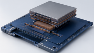
- Application to 2.5D/3D Packaging: Particularly in 2.5D packages, which connect multiple chips via an interposer, and 3D packages, which stack chips vertically, package warpage severely impacts manufacturing yield, electrical connections, and thermal management. Low warpage molding compounds ensure the stability of these complex structures.
- Improved Yield and Cost Reduction: Resolving the warpage issue facilitates wafer-level packaging and post-process handling, resulting in substantial improvements in manufacturing yield and reductions in production costs.
- Enhanced Thermomechanical Reliability: Stress relief within the package increases resistance to thermal cycling and thermal shock, reducing the risk of solder joint fatigue failure and delamination, thereby ensuring long-term device reliability.
Background & Context
With the evolution of AI, HPC, and 5G, the performance and integration density of semiconductor chips are accelerating. To meet these demands, 2.5D and 3D packaging technologies, which surpass the limits of conventional 2D packaging, are gaining attention. However, these advanced technologies face a significant challenge: due to the combination of materials with different thermal expansion coefficients and complex structures, packages are prone to substantial warpage during the manufacturing process. This warpage causes fine-pitch bonding failures, die-attach defects, and defects in downstream processes, becoming a major concern for the entire industry.
Strategic Significance & Outlook
The low warpage molding compound solutions showcased at IEEE ECTC 2026 are critically important for enabling the further proliferation and development of 2.5D/3D packaging technologies. This will accelerate the mass production of next-generation AI accelerators, data center processors, and high-performance GPUs, fueling the innovation these technologies bring to society. Moving forward, these materials are expected to continue evolving to meet reliability requirements under even harsher conditions and to support even finer packaging structures, becoming widely adopted as industry standards and strengthening the competitiveness of the entire semiconductor ecosystem.
Source: #
Get our weekly technology intelligence — free
Receive an infographic that lets you judge at a glance whether each field’s analysis report is worth reading.
Subscribe Free — Weekly Tech Intelligence
By subscribing, you’ll receive Troy-Technical’s weekly technology intelligence newsletter.
- Your email and selected fields are used only to deliver the newsletter.
- We never share your information with third parties.
- You can unsubscribe anytime via the link in each email.
See our Privacy Policy for details.
Takes about a minute · Unsubscribe anytime