Background
The relentless advancement of cutting-edge technologies—including Artificial Intelligence (AI), High-Performance Computing (HPC), autonomous vehicles, and 5G communications—is placing unprecedented demands on semiconductor chips across performance, power consumption, and form factor. As the rate of traditional CMOS scaling decelerates, the semiconductor industry is undergoing a profound paradigm shift, redefining packaging from a mere protective function to a primary enabler of system performance improvement and functional expansion. The discussions at SEMI Europe’s APC 2026 underscored this industry-wide transformation, signaling advanced packaging’s central role in innovation. Innovations in interconnects, enabling high-density power delivery and robust signal transmission, are especially critical for determining the power efficiency and throughput of modern AI accelerators.
Key Findings
The 2026 Advanced Packaging Conference (APC), organized by SEMI Europe, placed a central focus on innovations in power management and interconnect technologies—both indispensable for enabling high-performance AI systems. A key consensus emerged: as traditional device scaling, achieved through transistor miniaturization, approaches its physical and economic limits, advancements in advanced packaging (AP) and test technologies are now critical for sustaining system-level performance gains. Specifically, the conference highlighted 2.5D/3D integration, chiplet architectures, heterogeneous integration, and advanced substrate and interconnect technologies as pivotal for dramatically enhancing computing power, data bandwidth, and functionality, all while effectively reducing overall power consumption.
Technical Details
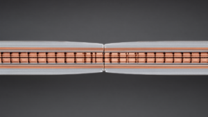
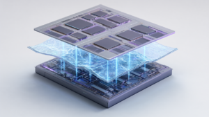
2.5D/3D integration technologies enable unprecedented integration density and performance by moving beyond the constraints of monolithic chips. This is achieved either by placing multiple semiconductor dies with diverse functionalities onto a silicon interposer (2.5D) or by stacking them vertically (3D). Chiplet architectures facilitate the construction of sophisticated System-on-Chips (SoCs) by assembling smaller, functionally specific ‘chiplets,’ thereby enhancing design flexibility, improving manufacturing yield, and reducing costs. Heterogeneous integration further optimizes system efficiency and performance by judiciously combining chiplets fabricated using disparate processes—such as logic, memory, analog, and RF components. These integrated approaches are vital for overcoming data movement bottlenecks and enhancing power efficiency in solutions like CoWoS (Chip-on-Wafer-on-Substrate), which integrates High Bandwidth Memory (HBM) directly with AI processors. Furthermore, advanced substrate technologies are instrumental in enabling fine-pitch wiring and low-loss signal transmission, which are critical for superior high-frequency characteristics and enhanced thermal management. Complementing these, precise interconnect technologies are paramount for ensuring signal integrity and long-term reliability within these increasingly complex packaging structures.
Strategic Significance & Outlook
Sustained innovation in advanced packaging and testing is an absolute imperative for future performance scaling in AI and HPC systems. Technologies such as 2.5D/3D integration, chiplets, and heterogeneous integration are poised for broader adoption and standardization in the coming years. This evolution will empower designers to efficiently construct increasingly complex and high-performance systems, thereby unlocking new applications and significant market opportunities. The strategic direction articulated at APC 2026 unequivocally signals the semiconductor industry’s commitment to prioritizing innovation in packaging and interconnects, charting a course towards a more sustainable and high-performance computing future.
Source: https://www.semiconeuropa.org/APC
Get our weekly technology intelligence — free
Receive an infographic that lets you judge at a glance whether each field’s analysis report is worth reading.
Subscribe Free — Weekly Tech Intelligence
By subscribing, you’ll receive Troy-Technical’s weekly technology intelligence newsletter.
- Your email and selected fields are used only to deliver the newsletter.
- We never share your information with third parties.
- You can unsubscribe anytime via the link in each email.
See our Privacy Policy for details.
Takes about a minute · Unsubscribe anytime