Key Findings
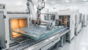
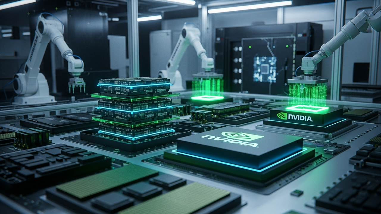
NVIDIA is accelerating the deployment roadmap for its next-generation Feynman AI platform, targeting a debut in late 2028. In response, TSMC is aggressively expanding its advanced packaging capacity, particularly for SoIC (System-on-Integrated-Chips) technology. Construction of the AP7 facility in Chiayi and AP8 in the Southern Taiwan Science Park is being expedited, with TSMC’s monthly SoIC production capacity projected to increase to approximately 50,000 wafers by the end of 2027.
Technical / Clinical Details
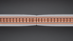
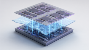
NVIDIA’s Feynman platform is designed to directly utilize TSMC’s cutting-edge A16 process and significantly increase the integration of SoIC 3D stacking and Co-Packaged Optics (CPO) technologies. SoIC represents TSMC’s advanced 3D chiplet technology, which involves vertically stacking multiple chiplets to substantially improve data transfer efficiency and power efficiency. CPO, by integrating optical interconnects directly within the package, dramatically enhances inter-chip communication speeds. These technologies are crucial for elevating AI chip performance to the next generation, and TSMC’s capacity expansion is a powerful enabler for NVIDIA’s innovative AI product launches.
Background & Context
The explosive growth in AI demand has created an unprecedented need for advanced packaging capacity within the semiconductor industry. AI accelerators, which require high-speed processing of vast amounts of data, are highly dependent on advanced packaging technologies like CoWoS (Chip-on-Wafer-on-Substrate) and SoIC. NVIDIA’s acceleration of the Feynman platform reflects intense competition in the AI market and the urgent need for more powerful AI infrastructure. TSMC’s capacity expansion is a strategic move to meet these market pressures and solidify its leadership in the AI semiconductor supply chain.
Strategic Significance & Outlook
TSMC is preparing capacity for a diverse range of advanced packaging solutions, including SoIC, CoWoS-L, and the next-generation CoPoS (Chip-on-Package-on-Substrate) technologies. The plan to increase SoIC monthly production capacity from 20,000 wafers by the end of 2026 to 50,000 wafers by the end of 2027 will significantly contribute to stabilizing the supply and enhancing the performance of future AI chips. This aggressive investment and technological development are expected to accelerate innovation in semiconductor back-end processes and potentially set new benchmarks for computing power in the AI era.
Get our weekly technology intelligence — free
Receive an infographic that lets you judge at a glance whether each field’s analysis report is worth reading.
Subscribe Free — Weekly Tech Intelligence
By subscribing, you’ll receive Troy-Technical’s weekly technology intelligence newsletter.
- Your email and selected fields are used only to deliver the newsletter.
- We never share your information with third parties.
- You can unsubscribe anytime via the link in each email.
See our Privacy Policy for details.
Takes about a minute · Unsubscribe anytime