Background
High Bandwidth Memory (HBM) technology has undergone significant evolution over the past 13 years, establishing itself as an indispensable component for accelerating AI chip performance. With the supply of GPUs and HBM for AI servers and data centers projected to remain constrained through 2026, the transition from HBM3E to HBM4 is an essential step to further enhance AI accelerator capabilities. Next-generation AI platforms, exemplified by NVIDIA’s Vera Rubin, are anticipated to exclusively require HBM4, driving specifications beyond current JEDEC standards. This robust market demand is accelerating plans for major HBM vendors—Samsung, SK Hynix, and Micron—to commence mass production of HBM4 between late 2025 and 2026.
Key Findings
HBM4, the forthcoming generation of High Bandwidth Memory, is set to redefine performance and efficiency benchmarks. It achieves this by doubling its I/O width from 1024 to 2048 bits, aiming for bandwidths exceeding 2.0 TB/s per stack. This monumental advancement is critically enabled by the adoption of hybrid bonding technology, which is projected to reduce thermal resistance by over 20% in 16-high stacks and enhance IOPS (Input/Output Operations Per Second) per Watt by up to 40% compared to its predecessor, HBM3E. HBM4 is therefore positioned as a pivotal solution to fundamentally alleviate data movement bottlenecks prevalent in artificial intelligence (AI) and high-performance computing (HPC) applications.
Technical and Market Details
As the sixth iteration of High Bandwidth Memory, HBM4 introduces a 2048-bit memory interface featuring 32 independent channels, representing the most significant architectural redesign in HBM history. This expanded interface facilitates lower operating frequencies relative to the immense bandwidth, leading to substantial improvements in power efficiency. A key shift involves the HBM4 base die migrating from mature logic nodes to advanced process nodes (N5/N3 class). Reports indicate SK Hynix is outsourcing its base die production to TSMC, while Samsung leverages its proprietary 4nm-class foundry, underscoring the industry’s commitment to cutting-edge process technology for HBM.
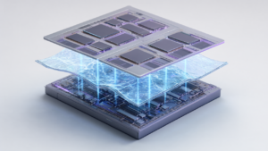
The most transformative technical innovation in HBM4 is its embrace of hybrid bonding (copper-to-copper bonding). This advanced interconnection method is implemented to effectively manage the increased heat generated by denser 16-high stack configurations. By eliminating physical gaps between dies, hybrid bonding significantly lowers thermal resistance, promising over 20% better heat dissipation compared to conventional micro-bump architectures. The stringent requirements for hybrid bonding necessitate extremely high precision, with surface flatness tolerances less than 1 nanometer, making meticulous process control paramount for achieving acceptable yields. Furthermore, HBM4 is engineered beyond a mere memory stack; it integrates logic dies to function as a co-processor, thereby augmenting the processing capability and flexibility of AI accelerators.
Strategic Significance and Outlook
The advent of HBM4 is poised to establish new benchmarks in AI and HPC system design, enabling the development of significantly higher-performance and more power-efficient systems. The ongoing maturation and widespread adoption of hybrid bonding technology will be instrumental in facilitating even higher HBM stacking and increased layer counts, with 16-high stacks anticipated to become standard for future HBM4E (mass production projected for 2027–2028). These comprehensive advancements promise tangible benefits, including reduced data center power consumption and accelerated AI model training times. Fundamentally, HBM4 is strategically positioned to alleviate critical bottlenecks in the AI semiconductor supply chain and drive further innovations in AI technology, cementing its increasing importance in the coming years.
Source: https://semihub.io/en/blog/hbm-guide-2.html
Get our weekly technology intelligence — free
Receive an infographic that lets you judge at a glance whether each field’s analysis report is worth reading.
Subscribe Free — Weekly Tech Intelligence
By subscribing, you’ll receive Troy-Technical’s weekly technology intelligence newsletter.
- Your email and selected fields are used only to deliver the newsletter.
- We never share your information with third parties.
- You can unsubscribe anytime via the link in each email.
See our Privacy Policy for details.
Takes about a minute · Unsubscribe anytime