Key Findings
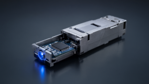
A report published by IMAPS 3D InCites concludes that silicon photonics, co-packaged optics (CPO), and advanced packaging technologies are indispensable for overcoming the computational and data transfer challenges posed by the explosive growth of large language models (LLMs) in data centers. The report specifically highlights efficient optical coupling between photonic dies and optical fibers as one of the most critical technical barriers in next-generation AI infrastructure, offering concrete approaches to resolve this challenge.
Technical / Clinical Details
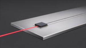
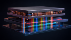
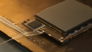
The report provides a detailed comparison of two primary methods for optimizing coupling between photonic dies and optical fibers: edge coupling and grating coupling. Edge coupling involves launching or extracting light from the chip’s facet, often achieving higher coupling efficiency but demanding precise alignment and dicing techniques. In contrast, grating coupling uses grating structures fabricated on the chip surface for light interaction, offering easier wafer-level testing and more relaxed alignment tolerances, though it may exhibit lower coupling efficiency compared to edge coupling. The choice between these technologies directly impacts packaging costs, manufacturing yield, and overall system performance. The report also suggests that combining these optical coupling techniques with advanced 3D packaging technologies like through-silicon vias (TSV) can maximize electrical and optical connection density between chips, leading to reduced power consumption and latency in data centers.
Background & Context
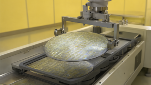
The exponential surge in AI workloads has dramatically escalated the demand for interconnect bandwidth within data centers. Traditional electrical wiring faces inherent physical limitations such as signal attenuation, power consumption, and heat generation, which now constitute a major bottleneck for data transfer between AI accelerators. In this context, optical interconnects are garnering significant attention as a solution capable of enabling faster and more energy-efficient data transmission. Silicon photonics, due to its compatibility with existing CMOS manufacturing processes, offers the potential for high-volume, low-cost production of optical devices, making it a pivotal technology for enhancing data center scale and performance.
Strategic Significance & Outlook
The convergence of advanced packaging technologies with silicon photonics and CPO is fundamental to shaping the future of AI computing. The continuous progress in these technologies will maximize the performance of AI accelerators, improve data center operational efficiency, and ultimately enable the creation of new AI applications. Specifically, optimizing coupling technologies between photonic dies and optical fibers will accelerate the adoption of optical interconnects, marking a crucial step towards realizing more high-performance and sustainable AI infrastructure. Investments and research and development in this sector are expected to remain robust, serving as the key to breaking computational barriers in the AI era.
Get our weekly technology intelligence — free
Receive an infographic that lets you judge at a glance whether each field’s analysis report is worth reading.
Subscribe Free — Weekly Tech Intelligence
By subscribing, you’ll receive Troy-Technical’s weekly technology intelligence newsletter.
- Your email and selected fields are used only to deliver the newsletter.
- We never share your information with third parties.
- You can unsubscribe anytime via the link in each email.
See our Privacy Policy for details.
Takes about a minute · Unsubscribe anytime