Background: The Challenge of Light Extraction and Miniaturization in Optics
For advanced technologies like LiDAR sensors, optical communication systems, and augmented reality (AR) devices, efficient control and extraction of light from integrated photonic chips are paramount. A long-standing challenge in silicon photonics has been the difficulty of efficiently coupling light from the confined waveguides on a chip into free space (and vice-versa) without relying on bulky external optics or mechanical moving parts. This limitation has historically constrained the miniaturization, reliability, and cost-effectiveness of light-based systems.
Key Findings: MIT’s Innovative Silicon Photonics Architecture
Researchers at MIT have developed a groundbreaking silicon photonics architecture that addresses this critical light-coupling challenge, paving the way for a new generation of compact and efficient optical devices. The core of their innovation lies in the use of precisely engineered microscopic curved structures:
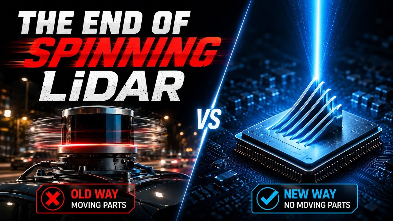
- Microscopic Curved Structures: The MIT team engineered minute, curved waveguide and antenna structures on a silicon photonics chip. These structures are specifically designed to efficiently scatter and direct light from the chip’s internal waveguides into a precisely controlled free-space beam. This eliminates the need for large external lenses, prisms, or mechanical gimbals to steer light.
- Efficient Free-Space Coupling: This novel design achieves high efficiency in light extraction and beam formation, minimizing energy loss as light transitions from the chip to the external environment. This efficiency is critical for both the power budget of devices and the signal-to-noise ratio in sensing applications.
- Solid-State and Compact Design: By integrating the light-steering mechanism directly onto the chip, the solution becomes entirely solid-state. This means no moving parts, leading to significantly enhanced reliability, durability, and a dramatic reduction in the overall size and weight of the optical system. This is a game-changer for applications where size and robustness are critical.
- Broad Application Potential: The architecture’s versatility suggests wide-ranging impact. For LiDAR, it enables smaller, more robust sensors for autonomous vehicles and drones. For optical communication, it could lead to more compact and efficient free-space optical links. In AR, it could facilitate the development of sleeker, lighter headsets with enhanced projection capabilities.
Technical Significance & Outlook: Reshaping Large-Scale Technologies
This MIT research is a powerful demonstration of how fundamental advancements at the microscopic level can trigger macroscopic transformations across entire technological sectors. Its significance stems from:
- Democratization of Optical Sensing: By significantly reducing the size, cost, and complexity of LiDAR and other optical sensors, this technology could democratize their use, enabling their integration into a far broader array of devices and systems.
- Enhanced Reliability and Energy Efficiency: The solid-state nature eliminates mechanical failure points, boosting reliability. Efficient light coupling reduces power consumption, extending battery life in portable devices and lowering operational costs in data centers.
- Fueling Future Innovation: Compact, efficient optical chips are a foundational component for next-generation AI, robotics, and human-computer interfaces. This breakthrough will enable new product designs and application possibilities previously deemed impractical.
The ability to precisely control and extract light from silicon photonics chips efficiently and compactly is a cornerstone for the future of ubiquitous 3D sensing, advanced communications, and immersive computing. This research solidifies the role of integrated optics as an indispensable enabler for the ongoing digital revolution.








Comments