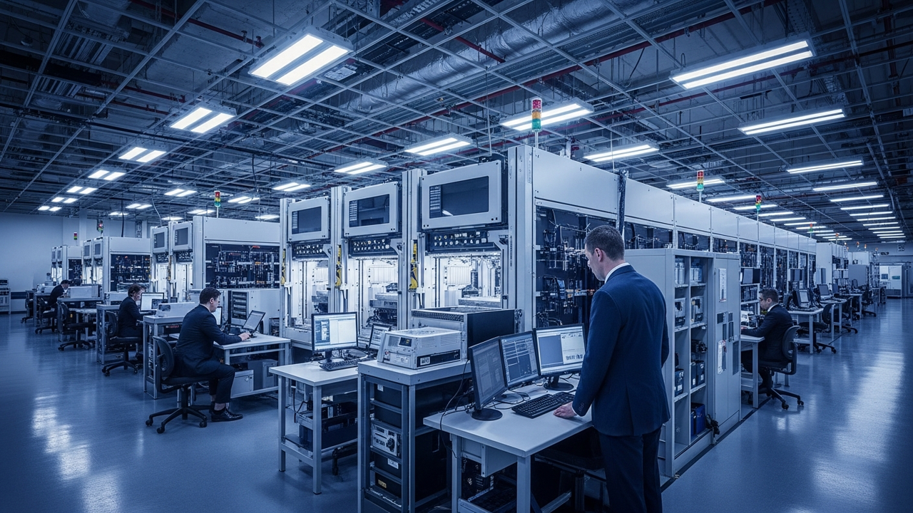
Background: Reinforcing U.S. Semiconductor Ecosystem
The U.S. government, through the CHIPS and Science Act, has initiated a concerted effort to onshore critical semiconductor manufacturing capabilities, particularly in advanced packaging. This strategic imperative aims to mitigate supply chain vulnerabilities, stimulate domestic innovation, and secure leadership in next-generation computing. Amkor Technology, a global leader in outsourced semiconductor assembly and test (OSAT) services, has emerged as a key player in this national initiative, demonstrating a robust commitment to enhancing U.S. manufacturing resilience.
Key Developments: Arizona Expansion and CHIPS Act Support
Amkor Technology announced a significant expansion of its U.S. operations by securing an additional 67 acres of land adjacent to its existing 104-acre campus in Peoria, Arizona. This move is part of a broader strategy to scale advanced packaging and test capabilities within the United States. Crucially, this expansion is bolstered by up to $407 million in direct funding from the U.S. Department of Commerce under the CHIPS Act. The new facility is projected to process approximately 14,500 wafers and 3.7 million units per month, addressing what has been identified as a “critical bottleneck” in 2.5D packaging technology. This capacity is vital for high-performance applications such as AI accelerators, high-performance computing (HPC), automotive electronics, and communications infrastructure, all of which rely heavily on advanced packaging solutions.
Technical Significance and Outlook
The establishment of this high-volume advanced packaging facility in Arizona is technically significant for several reasons. Firstly, it directly tackles the scarcity of domestic 2.5D packaging capacity, which is essential for integrating multiple chiplets into powerful, heterogeneous computing architectures. This allows for greater design flexibility, improved performance-per-watt, and enhanced thermal management – all critical factors for modern AI and HPC chips. Secondly, by establishing a state-of-the-art OSAT facility within the U.S., Amkor contributes to a more diversified and secure global semiconductor supply chain. The investment also supports the development of a highly skilled U.S. workforce in advanced packaging, fostering long-term innovation and competitiveness. As AI and HPC continue their exponential growth, Amkor’s expanded Arizona footprint is poised to be a cornerstone for realizing next-generation semiconductor technologies and ensuring U.S. leadership in advanced microelectronics manufacturing.









Comments