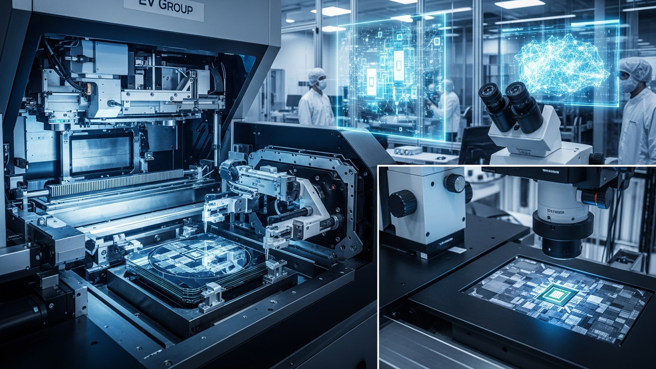
Background: The Imperative of Advanced Packaging and Heterogeneous Integration
As traditional Moore’s Law scaling encounters physical and economic limits, the semiconductor industry is increasingly relying on advanced packaging and heterogeneous integration to achieve higher performance, greater functionality, and improved power efficiency. This shift is particularly pronounced in the development of AI accelerators, high-performance computing (HPC) processors, and advanced memory solutions like HBM. These applications demand ultra-high interconnect density, minimal signal latency, and efficient thermal management, pushing the boundaries of conventional packaging techniques. EV Group, a leading supplier of wafer bonding and lithography equipment, is at the forefront of developing process solutions to meet these complex requirements.
Key Innovations and Product Offerings
At ECTC 2026, EV Group highlighted several key technologies designed to enable the next wave of semiconductor innovation:
- Hybrid Bonding (W2W and D2W): EV Group’s hybrid bonding solutions, including both wafer-to-wafer (W2W) and die-to-wafer (D2W) capabilities, facilitate direct, high-density electrical connections between stacked wafers or dies through dielectric layers and embedded metal pads. The company’s GEMINI® FB automated production wafer bonding platform is recognized as an industry standard, offering exceptional alignment and overlay accuracy critical for high-yield manufacturing of 3D NAND, DRAM, and HBM stacks.
- IR LayerRelease™ for Advanced Layer Transfer: This innovative technology utilizes an infrared laser to precisely debond and transfer ultra-thin semiconductor layers from a carrier substrate, such as sapphire. This capability is instrumental in creating novel device architectures, enabling material diversity, and facilitating the integration of different materials and functionalities in 3D-stacked devices, thereby expanding design flexibility for advanced integration.
- LITHOSCALE® XT Maskless Lithography: Addressing the need for flexible and cost-effective patterning in advanced packaging, LITHOSCALE® XT eliminates the reliance on expensive and time-consuming photomasks. This technology allows for rapid prototyping, design iteration, and efficient manufacturing of diverse chiplet designs and smaller-volume applications, accelerating the development cycle for heterogeneous integration.
The synergy of these technologies provides crucial pathways for achieving the stringent performance and integration demands of future semiconductor devices, with a strong emphasis on sub-micron level alignment accuracy and high-precision overlay metrology for D2W bonding.
Technical Significance and Market Outlook
EV Group’s portfolio directly addresses fundamental challenges in advanced semiconductor manufacturing. Hybrid bonding is pivotal for achieving the extreme interconnect densities required for modern AI and HPC chips, drastically reducing interconnect lengths and enhancing data transfer speeds while lowering power consumption. Layer transfer capabilities enable the creation of highly customized and complex 3D structures. Meanwhile, maskless lithography streamlines the R&D cycle, fostering rapid innovation in chiplet design and heterogeneous integration. These process solutions are not only critical for overcoming physical scaling limitations but also for enabling new product categories and market opportunities in AI, edge computing, and advanced connectivity, positioning EV Group as a foundational enabler for the next era of microelectronics.







Comments