Key Findings
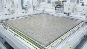
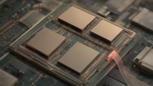
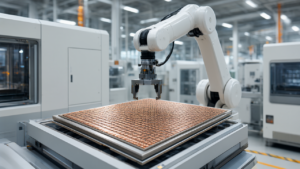
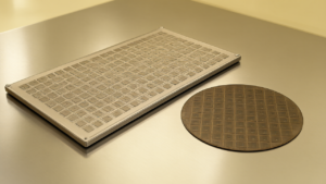
The industry is converging on the 510x515mm panel size, adopted by TSMC, Innolux, and Vogher, as it allows the reuse of mature G8.5 generation display production lines. While larger panels reduce costs and address capacity gaps—such as the estimated 300,000 to 400,000 unit shortage for CoWoS in 2026—they introduce exponential risks in warpage and yield. Consequently, AI chips with tight RDL requirements (1-10μm) remain on more conservative sizes, while PMIC and RF chips (10-20μm) are targeted for larger panels exceeding 600mm.
Technical Details: The Warpage Wall
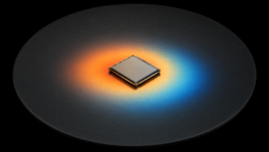
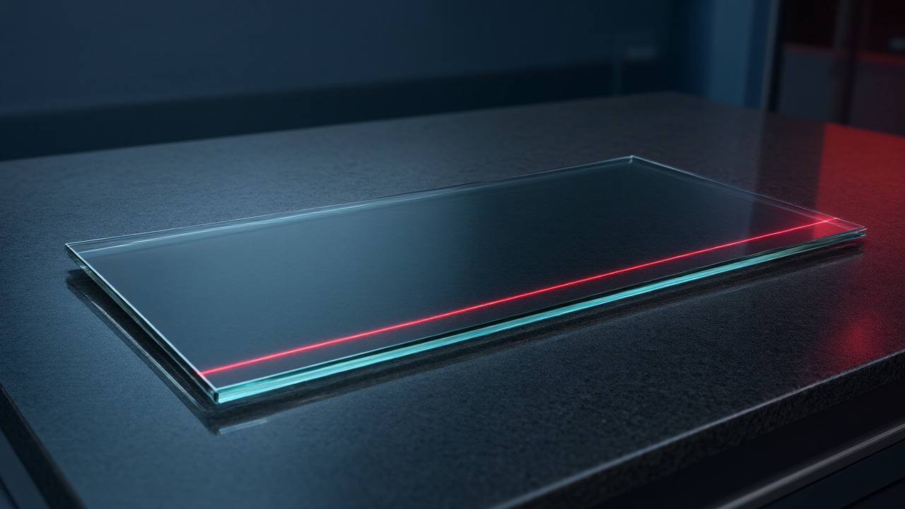
Warpage is driven by the difference in coefficients of thermal expansion (CTE) between materials: silicon (~2.6 ppm/℃), copper (16-17 ppm/℃), and organic dielectric layers (30-60 ppm/℃). According to thin-plate mechanics, warpage displacement (w) is proportional to the square of the characteristic length (L²). Increasing a panel from 300mm to 600mm quadruples the warpage driving force, which can lead to focus errors in stepper exposure machines and mechanical handling failures.
To mitigate this, the industry employs three strategies:
- Material: Using low-CTE glass (3.2 to 7.2 ppm/℃) to match silicon, though this increases brittleness and costs by 30-50%.
- Structure: Implementing symmetrical routing (e.g., TSMC’s CoPoS) to cancel out local stress.
- Process: Utilizing air gaps, stress buffer layers, or “chip-after” RDL sequences to reduce thermal stress.
Industry Roadmap and Adopters
TSMC’s CoPoS roadmap targets mass production between 2028 and 2029, with 510mm as a mid-term goal. Intel is pursuing a more aggressive 510x515mm route with 24-layer glass cores. In China, BOE has invested 993 million yuan in a test line with a monthly capacity of 1,000 pieces, while Vogher reports a TGV monthly capacity of 10,000 pieces based on the 510x515mm size. Other players include Samsung Electro-Mechanics (415x510mm) and Rapidus (600x600mm).
Significance and Outlook
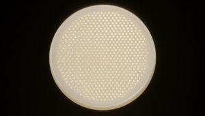
The transition from circular wafers to square panels is a strategic move to solve capacity shortages for AI GPUs, such as the Nvidia Rubin generation. However, because total panel yield is the product of individual hole yields, increasing the area exponentially increases the risk of failure. The upper limit of panel size is effectively defined by the limit of warpage control.
Source: https://finance.sina.com.cn/wm/2026-10-27/doc-iniwrzht4588328.shtml
Get our weekly technology intelligence — free
Receive an infographic that lets you judge at a glance whether each field’s analysis report is worth reading.
Subscribe Free — Weekly Tech Intelligence
By subscribing, you’ll receive Troy-Technical’s weekly technology intelligence newsletter.
- Your email and selected fields are used only to deliver the newsletter.
- We never share your information with third parties.
- You can unsubscribe anytime via the link in each email.
See our Privacy Policy for details.
Takes about a minute · Unsubscribe anytime