New Technology– category –
-

Lam and imec: 3D Integration and High-NA EUV Roadmap for AI
Electronics Weekly UK Overview Lam Research and imec are collaborating to accelerate the transition of 3D integration and advanced patterning technologies from the lab to high-volume manufacturing. The partnership focuses on solving proc... -
Hunan Titan Future: China’s First 12-Inch Polycrystalline SiC Substrate
TrendForce News China Overview Hunan Titan Future Technology has developed China's first 12-inch polycrystalline silicon carbide (SiC) substrate featuring thermal conductivity exceeding 280 W/(m·K). Designed for AI computing chips and ad... -
Photosensitive Crystallizable Glass: KICET’s TGV Process for Semiconductors
Financial News (파이낸셜뉴스) South Korea Overview The Korea Institute of Ceramic Technology (KICET) has developed a photosensitive crystallizable glass material to enable the domestic production of next-generation semiconductor substrat... -
GIST Glass Substrates: Low-Dielectric Material for AI Chips
Money Today (mt.co.kr) South Korea Overview Researchers at the Gwangju Institute of Science and Technology (GIST) have developed a low-dielectric aluminoborosilicate glass material to replace polymer-based organic substrates in AI semico... -
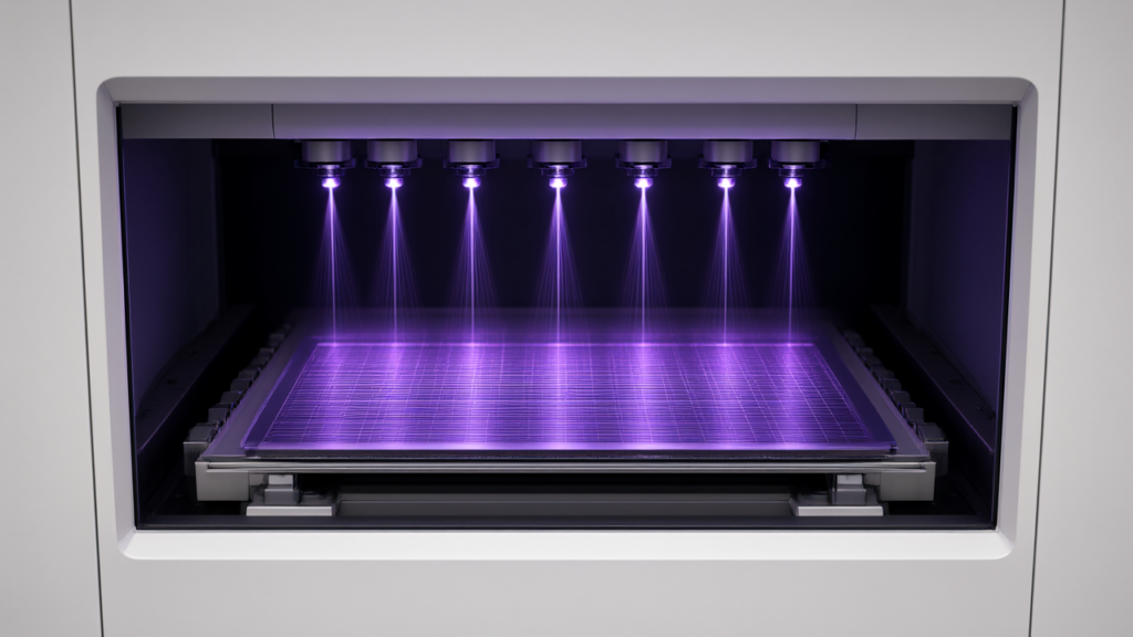
Nikon DSP-110: Specs and Timeline for 1.5μm Digital Exposure
MONOist(ITmedia) Japan Overview Nikon will release the DSP-110 digital exposure system for advanced semiconductor packaging in April 2027, featuring a resolution of 1.5μm. The system increases throughput by approximately 40% compared t... -
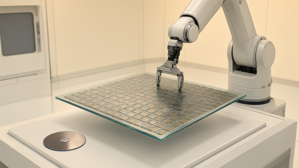
Panel-Level Packaging: Scaling Challenges vs Wafer-Level Flow
Semiconductor Engineering USA Overview Transitioning advanced packaging from 300mm wafers to larger panels significantly increases unit yield for large AI and HPC packages, with some configurations producing 8 times more units than wafer... -
Groq AI Chips: Shift to 3D-Stacked DRAM for Memory Capacity
TrendForce Taiwan Overview Groq is considering a transition from SRAM-centric designs to 3D-stacked DRAM for its next-generation AI chips to address the widening gap between memory capacity and AI model growth. This shift aims to increas... -
NVIDIA Vera CPU: Monolithic Die Architecture vs x86 Performance
TrendForce Taiwan Overview NVIDIA has opted for a monolithic compute die for its Vera CPU to optimize for agentic AI, claiming up to 2× the performance of leading x86 processors in sequential tasks. The architecture prioritizes low laten... -
Photonics-Electronics Convergence: NEDO Project for AI Chiplets
NTT Group Japan Overview NTT Innovative Devices leads a four-company consortium selected by NEDO to develop mass-production technologies for photonics-electronics convergence (PEC) devices. The project targets a tenfold increase in manuf... -
CIT ASEDep: Single-Crystal Copper Deposition for AI Packaging
(No explicit source, appears to be a press release repost) South Korea Overview CIT has introduced ASEDep, a manufacturing solution for semiconductor packaging substrates that utilizes single-crystal copper deposition. The technology aim...