Key Findings
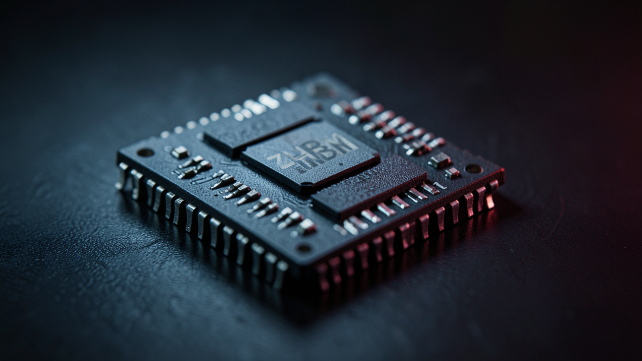
Samsung is pioneering a concept called ‘zHBM,’ a next-generation memory technology poised to revolutionize high-bandwidth memory (HBM) architectures by directly stacking DRAM onto the processor rather than relying on an interposer. This innovative approach is projected to achieve approximately 70% lower I/O power consumption compared to HBM5 and deliver 2.3 times the bandwidth of HBM4E. Such an advancement promises significant improvements in performance and power efficiency, particularly for edge AI devices.
Technical / Clinical Details
The core of the zHBM technology lies in wafer-on-wafer hybrid copper bonding. This method enables direct, fine-pitch electrical connections between chips, offering higher density and superior electrical characteristics than traditional thermocompression bonding with microbumps. However, realizing zHBM requires unprecedentedly close co-design efforts between DRAM and System-on-Chip (SoC) teams, elevating the level of memory-logic integration. Jaesik Lee, VP of Packaging Engineering at SK hynix, commented that hybrid bonding technology is not yet mature for the HBM4E generation, anticipating its earliest viable adoption will be with HBM5, which necessitates 20-layer DRAM stacking.
Background & Context
The exponential growth in AI processing demands has made memory bandwidth and power efficiency critical bottlenecks, especially in edge AI devices and data centers. While HBM emerged to address these challenges, the continuous push for higher performance and lower power consumption necessitates further innovation. Conventional HBM connects to processors via an interposer, leading to longer signal paths, power loss, and latency. zHBM seeks to fundamentally resolve these issues by eliminating the interposer.
Strategic Significance & Outlook
Direct stacking technologies, with hybrid bonding at their core, like zHBM, have the potential to profoundly impact future edge AI chip designs, enabling the development of smaller, more efficient, and higher-performing AI devices. However, achieving high-precision wafer-level bonding, fostering close collaboration across different vendors, and establishing new design and manufacturing processes will require several more years of development. Anticipated for adoption with the HBM5 generation, this technology represents a crucial milestone that will further drive innovation in the semiconductor back-end industry.
Get our weekly technology intelligence — free
Receive an infographic that lets you judge at a glance whether each field’s analysis report is worth reading.
Subscribe Free — Weekly Tech Intelligence
By subscribing, you’ll receive Troy-Technical’s weekly technology intelligence newsletter.
- Your email and selected fields are used only to deliver the newsletter.
- We never share your information with third parties.
- You can unsubscribe anytime via the link in each email.
See our Privacy Policy for details.
Takes about a minute · Unsubscribe anytime









Comments