TECHNOLOGY EXPLAINER
What a Glass Substrate Is
— changing the foundation of a chip package from resin to glass
For nearly thirty years the foundation under a semiconductor has been organic resin. The effort to replace that assumption is now in earnest — and sitting at the centre of the development race are Japan's glass makers. This article is written to be readable both for newcomers and for materials engineers.
- What a glass substrate is (the short version)
- Why it became necessary — where resin runs out
- The four things glass brings
- TGV — how do you get holes through glass?
- A materials engineer's view: CTE becomes something you design
- Glass ceramic as an answer
- Panel size as the ground the race is fought on
- Who is developing it
- What is still hard — glass breaks
- What comes next (the timing is not settled)
- Glossary / Primary sources / Claim-to-source audit
Sourced = a value stated in published material from a research institute or manufacturer (link given)
Our calculation = a figure this article derived, with the assumptions spelled out
Not yet confirmed = a target or a plan with no confirmed production record
Press report = reported by trade media, and not verified in an official announcement by the manufacturer
1. What a glass substrate is (the short version)
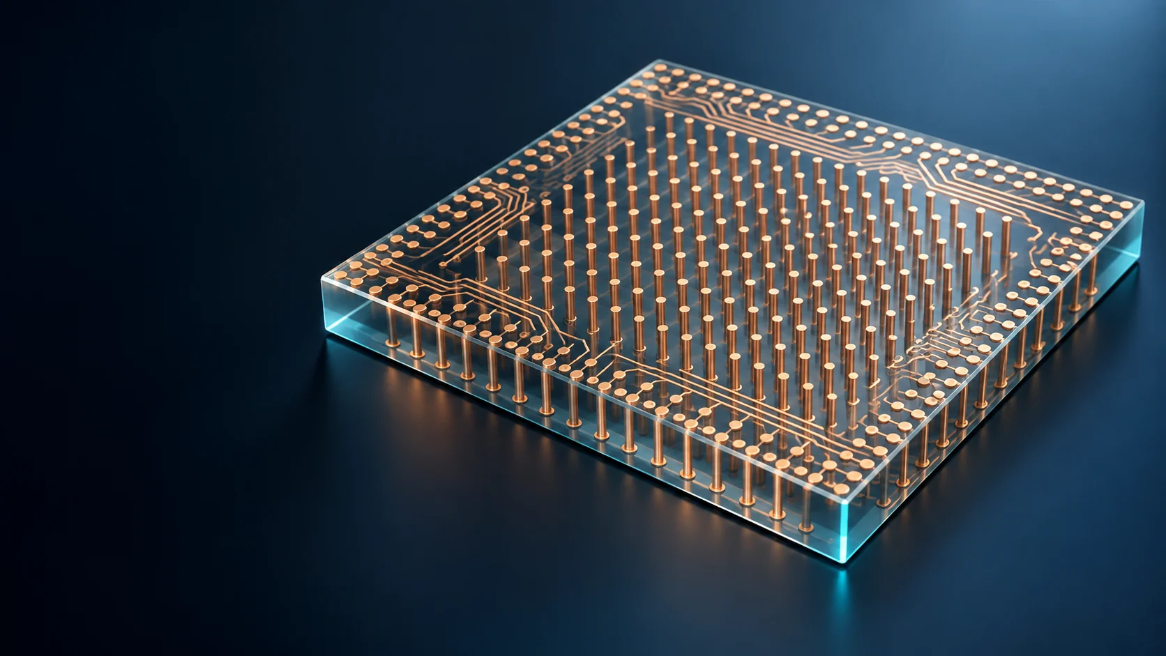
A glass substrate, in this context, means a package substrate whose central core layer has been changed from resin to glass. It is also called a glass core substrate.
- Only the core layer changes: the whole substrate does not become glass. The stiff plate at the centre does.
- Build-up layers stay as they are: the stacked resin and copper wiring layers above and below remain.
- The holes are TGVs: through-glass vias carry the connections from one face to the other.
In the package substrate article we described the core layer as the part that supplies stiffness and flatness. We also saw that, as AI packages grow, warpage has become the factor that decides reliability and yield. A glass substrate is an attempt to hand that job to a material that can do it better.
2. Why it became necessary — where resin runs out
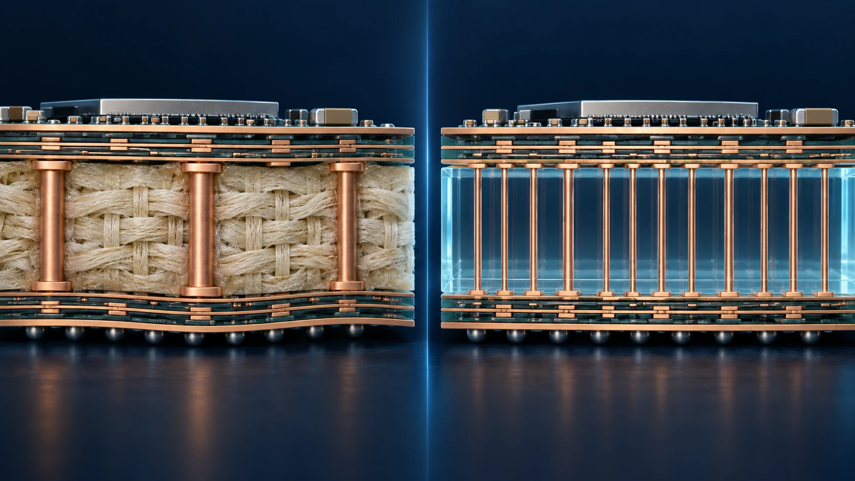
Intel put the problem bluntly in its announcement of 18 September 2023 Sourced.
By the end of this decade, the semiconductor industry is likely to reach the limits of transistor integration in packages built on organic materials, which carry penalties in power consumption and limits in shrinkage and warpage (Intel).
AT&S says much the same thing: conventional organic laminates are running into limits on three fronts — warpage, line and space scaling, and dielectric loss Sourced (AT&S).
Put plainly: finer wiring, bigger packages, faster signals — resin can no longer deliver all three demands at the same time.
3. The four things glass brings
The advantages Intel lists are not a flat list. They form a chain, where one property makes the next one possible. Following them in order is the easiest way to see the logic.
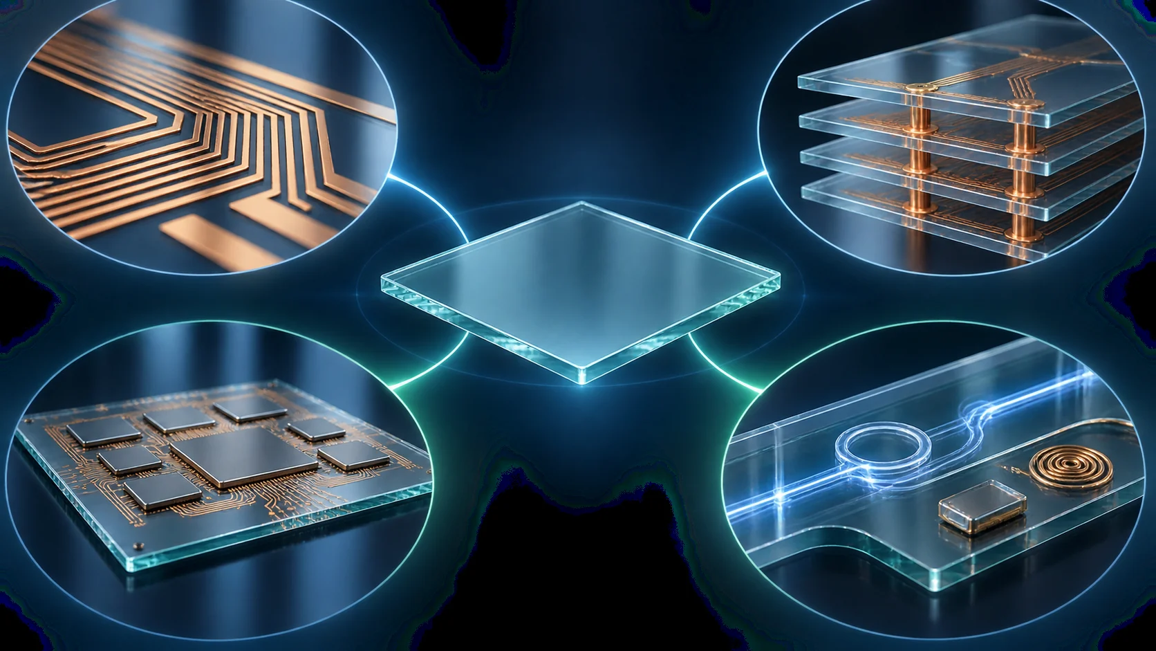
Intel describes the substrate as the result of a decade of research, and names its first landing zones as applications that need large packages — data centre, AI and graphics — together with high-speed uses Sourced.
4. TGV — how do you get holes through glass?
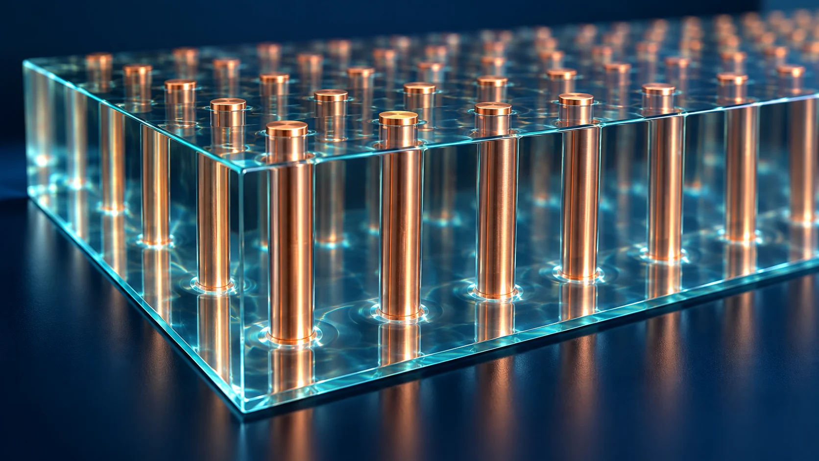
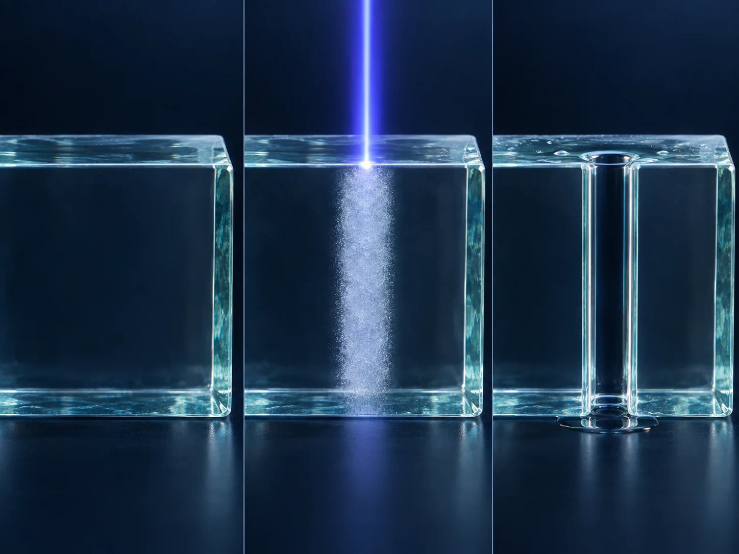
The technical heart of a glass substrate is, in practice, the drilling. Connecting the two faces requires an electrode that runs right through the plate: a TGV, or through-glass via.
And glass is a material that cracks when you try to put a hole in it. How each company solves that is where their technologies diverge.
Two routes
Nippon Electric Glass has developed products for both ways of forming a TGV, and describes the character of each as follows Sourced (Nippon Electric Glass, 22 May 2025).
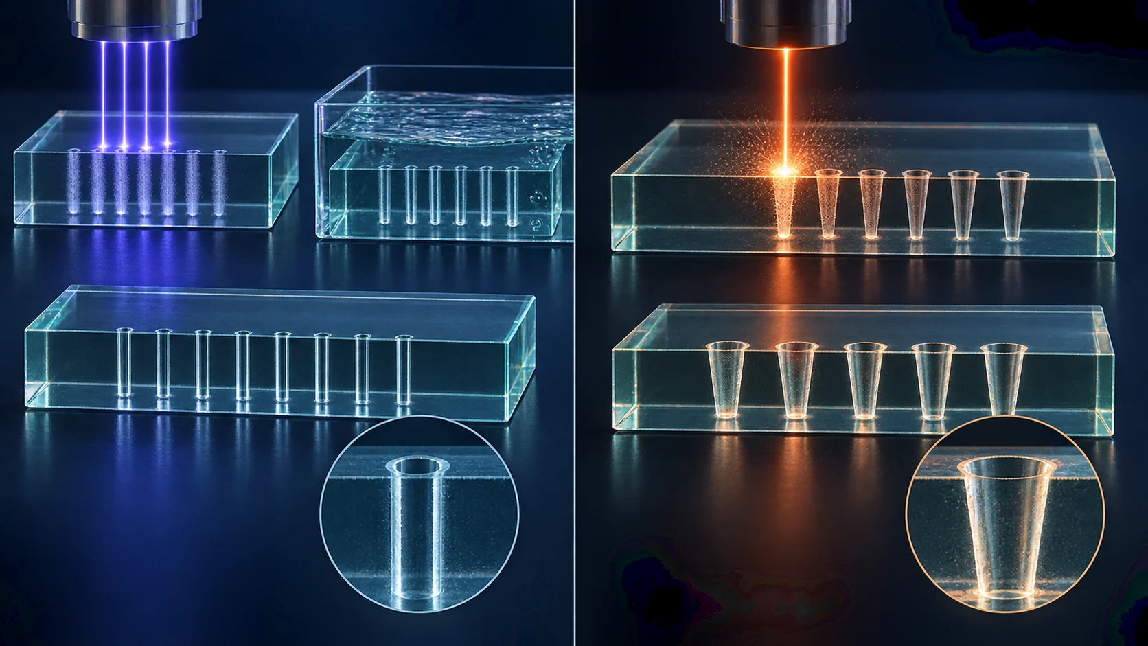
Route 1, laser modification followed by etching, changes only the character of the material with a laser and then dissolves that part in a chemical bath. The idea is to create a soluble region without breaking the glass, and it is what makes the fine holes possible.
Route 2, the CO₂ laser, looks like brute force, but its value lies elsewhere: the laser tools already installed for printed circuit boards can be used as they are. Nippon Electric Glass makes exactly this point, saying the route keeps capital spending down Sourced.
Performance alone does not decide whether a new material spreads. How much of the existing production equipment can be carried over governs how fast it gets adopted. The fact that both routes are being developed in parallel reflects that practical reality.
After the hole — metallisation
Once the hole exists, metal has to go into it. AT&S describes two options — full copper fill, and sidewall plating with a dielectric fill — and notes that each carries a different trade-off between stress and reliability Sourced.
AGC states that it can form fine TGVs of 50 µm diameter and above accurately, at tight pitch, and that it supports high aspect ratios, up to 20:1 in a 1.0 mm thick plate Sourced (AGC).
5. A materials engineer's view: CTE becomes something you design
This, to my mind, is the most interesting part of the whole technology.
In an organic core material the coefficient of thermal expansion is largely fixed once you have chosen the resin and the glass cloth. With glass, CTE can be designed by changing the composition.
| Manufacturer | What they have published |
|---|---|
| Nippon Electric Glass | Several grades offered as inorganic core substrates. CTE 6.1 to 8.9 ppm/°C, flexural strength 150 to 340 MPa. Reduced dimensional change and warpage at high temperature and high humidity |
| AGC | CTE can be tuned to optimise stress. High elastic modulus for warpage control. Plate thickness from 0.1 to 1.1 mm and beyond |
| AT&S | The coefficient of thermal expansion can be designed close to that of silicon, reducing thermomechanical stress and warpage during assembly and thermal cycling |
| Samsung Electro-Mechanics | Compared with conventional organic substrates, lower thermal expansion and better flatness |
All Sourced (published material from each company).
Inside a package the core substrate is sandwiched between two things that behave very differently: the silicon die, which barely expands, and the motherboard, which expands a lot. Which of the two you match determines where the stress concentrates.
Nippon Electric Glass offers three grades — low dielectric constant, high expansion and high strength — precisely because the best answer differs by application Sourced. Prioritise high-speed signalling and you take the low-dielectric grade; prioritise the stress balance against the board below and you take the high-expansion grade; want to avoid cracking during processing and assembly and you take the high-strength grade.
The material itself becomes a design variable. That is a degree of freedom organic core materials never had. It also means the material maker tailors the composition customer by customer, which puts a glass maker's accumulated know-how directly on the critical path.
6. Glass ceramic as an answer
On 15 January 2025 Nippon Electric Glass announced GC Core™, a glass ceramic core substrate made from a composite of glass powder and ceramic powder Sourced.
What this material addresses is exactly the problem raised in section 4: glass cracks when you drill it. The company says GC Core allows fast, crack-free drilling with a standard CO₂ laser tool, and that because it can be matched to the specifications of existing semiconductor production equipment it keeps capital spending down Sourced (Nippon Electric Glass).
Pure glass is homogeneous, and that is the problem: once a crack starts, nothing stops it propagating. Disperse ceramic particles through it and a crack runs into a particle, is deflected, and spends energy doing so — the standard toughening mechanism of a composite material Commentary.
The point worth noticing is that both the resistance to cracking and the ease of machining are being solved in the composition of the material itself. Rather than making the equipment cleverer to avoid breakage, you make a material that does not break. It is a textbook case of the material side absorbing a process constraint.
7. Panel size as the ground the race is fought on
Alongside performance, the other axis of competition in glass substrates is how large a plate you can build on.
For GC Core, Nippon Electric Glass announced a 300 mm square format in June 2024, then in January 2025 a large panel size of 515 × 510 mm at 1.0 mm thickness Sourced. AT&S also lists as an advantage that, unlike a silicon interposer, glass can be formed in the large panel sizes that suit advanced packaging lines Sourced.
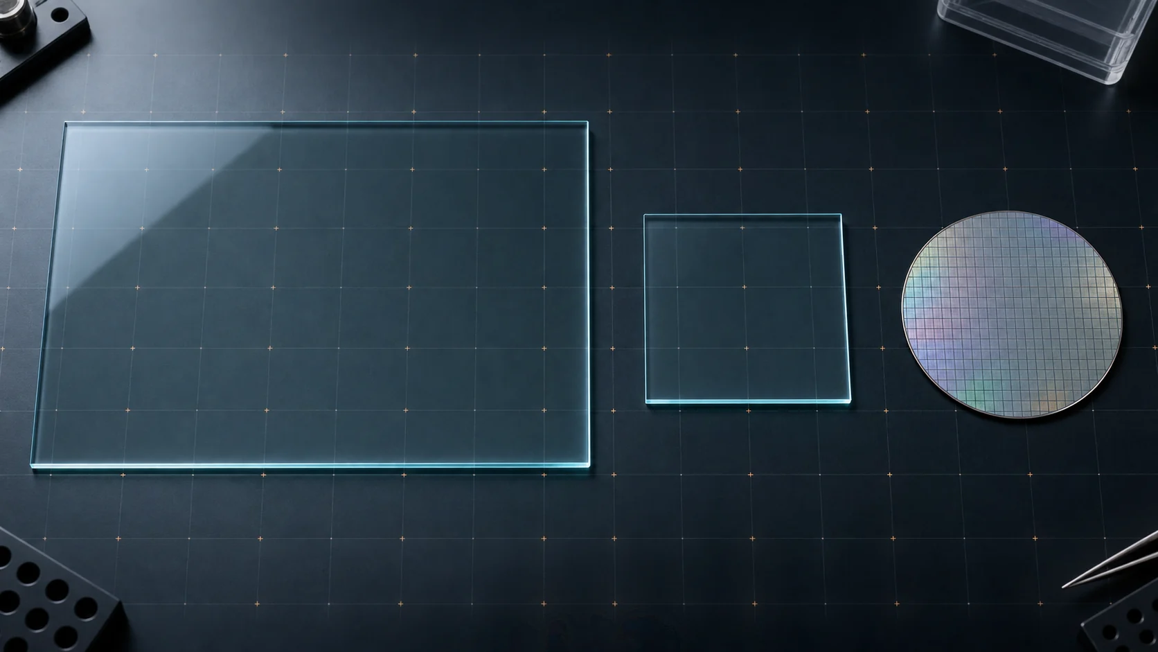
515 × 510 mm works out at about 262,650 mm², roughly 3.7 times the area of a 300 mm wafer Our calculation. The more area you can process in one pass, the lower the manufacturing cost per piece. A silicon interposer is tied to a round wafer; glass can be made as a large rectangular panel — which is an advantage in area efficiency as well.
8. Who is developing it
| Company | Published activity | Date |
|---|---|---|
| Intel | Announced what it calls industry-leading glass substrates, the result of a decade of research. Market introduction planned for the second half of this decade | September 2023 |
| Nippon Electric Glass | Developed 515 × 510 mm TGV glass core substrates. The grade for laser modification and etching is already sampling; development continues on the CO₂ laser grade | May 2025 |
| AGC | Thickness 0.1 to 1.1 mm and above, fine TGVs of 50 µm and up, aspect ratio to 20:1. Aimed at 3D packaging, chiplets, CPO substrates and RF devices | — |
| AT&S | Glass core is a focus of its IC substrate competence centre in Leoben, Austria. Working with semiconductor makers on prototype development | — |
| Samsung Electro-Mechanics | Signed an MOU with the Sumitomo Chemical group (Dongwoo Fine-Chem) to set up a joint venture for glass core manufacturing, with Dongwoo Fine-Chem's Pyeongtaek site as the initial production base | November 2025 |
All Sourced (published material from each company).
What stands out in that list is that the Japanese names are on the material side. Nippon Electric Glass and AGC supply the glass itself; the Sumitomo Chemical group joins the Korean venture. Just as with ABF (Ajinomoto) in the package substrate article, and photosensitive polyimide and PBO (HD MicroSystems, JSR, Sumitomo Bakelite) in the RDL article, Japanese companies are deeply embedded in the material layer of advanced packaging.
9. What is still hard — glass breaks
The weakness of glass is one anyone can grasp intuitively. It breaks. And that is genuinely the central problem in development today.
Intel lists three practical obstacles to making glass substrates work Sourced (Intel, November 2023).
- Making the edges resistant to breakage
- How to singulate a sheet of substrates into individual pieces
- Simply how to protect and handle the material
On the technical side the listed questions are which glass is best, how to stack the metals and devices on it, how to drill the fine holes and run the wiring through them, and how to make it survive heat and mechanical force across the life of the product Sourced.
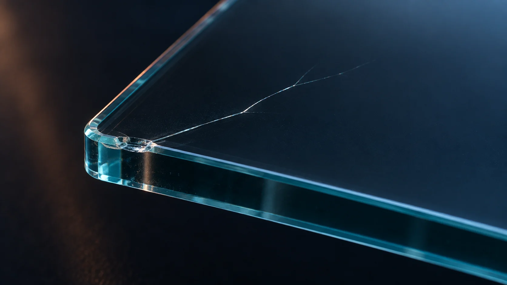
The strength of glass is set less by the strength of the material itself than by the flaws on its surface and edges. So the problem spans not only the composition but cutting, polishing, cleaning and handling as well. Read in that light, the range Nippon Electric Glass quotes for flexural strength — 150 to 340 MPa across three grades — starts to mean something.
10. What comes next (the timing is not settled)
Nippon Electric Glass: for the CO₂-laser-compatible inorganic core substrate, it has stated that it
aims to begin mass production in 2028 Sourced.
Samsung Electro-Mechanics: targets a definitive joint-venture agreement the following year, with
mass production from 2027 at the earliest. Prototyping is currently done at the Sejong plant
Sourced.
Intel: as of September 2023, plans market introduction in the second half of this decade
Sourced.
As of our research date of September 2026, we found no official announcement from any manufacturer declaring that mass production of glass core substrates had begun Not yet confirmed. The companies read as being at the prototype, sampling and customer-evaluation stage.
Trade media report actively on each company's production timing, but they do not agree with one another Press report. Nor could we find any later official Intel statement confirming or revising the second-half-of-the-decade plan it set out in 2023.
If you cover this topic in a technical explainer, we would suggest keeping each company's targets and its track record clearly separate.
11. Glossary
- Glass core substrate
- A package substrate whose core layer has been replaced by glass, with build-up layers above and below.
- Core layer
- The thick layer at the centre of the substrate. It carries the stiffness and flatness.
- TGV
- Through-glass via. An electrode that runs through the glass to connect front to back.
- Laser modification
- Changing only the character of the glass inside the plate with a laser, then dissolving that region in a chemical bath to leave a hole.
- CO₂ laser drilling
- Removing glass directly with a laser to open a hole. Existing PCB equipment can be used.
- Aspect ratio
- The ratio of hole depth to diameter. Higher means a narrower, deeper hole.
- CTE
- Coefficient of thermal expansion. Differences between materials create warpage and stress. In glass it can be tuned by composition.
- TTV
- Total thickness variation. How much the plate thickness varies. Smaller means flatter.
- Flexural strength
- How much bending a plate withstands. In glass it depends heavily on surface and edge flaws.
- Glass ceramic
- A composite of glass and ceramic. Cracks propagate through it less readily.
- Dissipation factor
- The fraction of signal energy that turns into heat. Lower is better for high-speed signals.
- CPO
- Co-packaged optics. Integrating optical components into the package. The transparency of glass becomes useful here.
- Singulation
- Cutting a large plate into individual product pieces. With glass it is a leading cause of breakage.
- Panel level
- Manufacturing on a large rectangular panel rather than a round wafer. Better area efficiency.
12. Primary sources
- Intel "Intel Unveils Industry-Leading Glass Substrates to Meet Demand for More Powerful Compute", 18 September 2023 — intel.com
- Intel "In Glass, a View to the Future of Powerful Chips", 16 November 2023 — newsroom.intel.com
- Nippon Electric Glass "Development of large TGV glass core substrates for laser-modification-and-etching and for CO₂ laser processing", 22 May 2025 (Japanese-language release) — neg.co.jp
- Nippon Electric Glass "Development of GC Core™, a glass ceramic core substrate in a 515 x 510 mm large panel size", 15 January 2025 (Japanese-language release) — neg.co.jp
- Nippon Electric Glass "What is an inorganic core substrate for semiconductor packages?", product information (Japanese-language page) — neg.co.jp
- AGC "CES 2026: semiconductor-related solutions" — agc.com
- AT&S "Glass Core Substrates: From R&D breakthrough to platform technology" — ats.net
- Samsung Electro-Mechanics "Signs MOU with Sumitomo Chemical Group to Establish a Joint Venture for 'Glass Core'", 5 November 2025 — samsungsem.com
13. Claim-to-source audit
| Claim in the text | Basis | Label |
|---|---|---|
| Organic materials carry a power penalty and limits in shrinkage and warpage, and integration on them is likely to reach its limit by the end of the decade | Intel press release, 18 September 2023[Source 1] https://www.intel.com/content/www/us/en/newsroom/news/intel-unveils-industry-leading-glass-substrates.html | Sourced |
| Glass offers ultra-low flatness deviation, high-temperature tolerance and dimensional stability; pattern distortion is cut by 50% and wiring density can rise tenfold; improved mechanical properties give high assembly yield even on very large packages; optical interconnect and embedded inductors and capacitors become possible; the goal is one trillion transistors in a package by 2030 | Intel press release, 18 September 2023[Source 1] https://www.intel.com/content/www/us/en/newsroom/news/intel-unveils-industry-leading-glass-substrates.html | Sourced |
| Intel describes a decade of research, with first adoption in large form factors (data centre, AI, graphics) and high-speed applications | Intel press release, 18 September 2023[Source 1] https://www.intel.com/content/www/us/en/newsroom/news/intel-unveils-industry-leading-glass-substrates.html | Sourced |
| The obstacles Intel lists: edge breakage, singulation, protection and handling, which glass is best, stacking, fine holes and wiring, and surviving heat and mechanical force | Intel article, 16 November 2023[Source 2] https://newsroom.intel.com/new-technologies/in-glass-view-future-of-powerful-chips | Sourced |
| Organic laminates are limited on warpage, line and space scaling and dielectric loss; glass CTE can be designed close to silicon and formed in large panels; TGV metallisation by full copper fill or sidewall plating with dielectric fill carries different trade-offs | AT&S technical article[Source 7] https://ats.net/en/glass-core-substrates-from-rd-breakthrough-to-platform-technology/ | Sourced |
| Nippon Electric Glass: two TGV routes (laser modification and etching, 50 µm via in 0.4 mm glass; CO₂ laser, 90 µm via in 0.5 mm glass), compatibility with existing PCB laser tools, 515 x 510 mm, and the aim of starting mass production in 2028 | Nippon Electric Glass news release, 22 May 2025[Source 3] https://www.neg.co.jp/news/20250522-1.html | Sourced |
| GC Core: a composite of glass powder and ceramic powder, 515 x 510 mm at 1.0 mm thick, fast crack-free drilling with a standard CO₂ laser, reduced capital spending, and the 300 mm square format announced in June 2024 | Nippon Electric Glass news release, 15 January 2025[Source 4] https://www.neg.co.jp/news/20250115.html | Sourced |
| Inorganic core substrates: CTE 6.1 to 8.9 ppm/°C, flexural strength 150 to 340 MPa, and three GC Core grades (low dielectric constant, high expansion, high strength) | Nippon Electric Glass product page[Source 5] https://www.neg.co.jp/products/inorganic-core-substrate/index.html | Sourced |
| AGC: thickness 0.1 to 1.1 mm and above, fine TGVs of 50 µm and up, high aspect ratio (to 20:1 in 1.0 mm thick glass), tunable CTE, high modulus for warpage control, aimed at 3D packaging, chiplets, CPO substrates and RF devices | AGC published page[Source 6] https://www.agc.com/ces/semiconductor.html | Sourced |
| Samsung Electro-Mechanics signed an MOU with the Sumitomo Chemical group (Dongwoo Fine-Chem) for a glass core joint venture; mass production from 2027 at the earliest, with prototyping at the Sejong plant; glass core has lower CTE and better flatness than organic substrates | Samsung Electro-Mechanics announcement, 5 November 2025[Source 8] https://samsungsem.com/global/newsroom/news/view.do?id=9850 | Sourced |
| 515 x 510 mm = about 262,650 mm²; a 300 mm wafer = about 70,686 mm²; an area ratio of about 3.7 | Our calculation from 515 x 510 and from π × 150² | Our calculation |
| The mechanism by which a composite resists crack propagation, and the point that the strength of glass depends on surface and edge flaws | Commentary based on general relationships in materials engineering. No numerical claim is made about any specific product | Commentary |
| The start of mass production of glass core substrates | No manufacturer declaration of mass production could be confirmed as of the research date for this article, and trade-media reports do not agree | Not yet confirmed |
Last updated 20 September 2026. Sources are limited to primary material (official announcements and product pages from the manufacturers). All figures are explanatory concept graphics. Visual-overview figures are shown as AI-generated conceptual images, matching the Japanese edition. Vector drawings are retained where they carry quantitative values or precision-critical technical labels. AI-generated images do not depict real equipment, products, facilities, dimensions or exact cross-sections; replaced source SVG overview drawings remain in the HTML but are hidden.