COMPANY PROFILE / SEMICONDUCTOR BACK-END
TSMC
The front-end company that became the biggest player in back-end packaging
TSMC is the world's largest pure-play foundry: it manufactures chips that other companies design. Yet what now governs the supply of AI silicon is not the transistors it builds in the front end but its advanced packaging capacity, above all CoWoS. This profile traces how a "wafer company" ended up at the centre of the back end, using only numbers the company has published itself.
- TSMC in 30 seconds
- The logo and how the name is written
- What the company actually does: the foundry model
- Scale: five years of revenue
- Company category and position in the back-end industry
- Sites and the countries where it manufactures
- Leading products and share in semiconductor back-end work
- Current investment plans
- Major corporate partners
- Where the company is heading in this field
- The risks this company carries
- Glossary, references and claim-to-source audit
1. TSMC in 30 seconds
New York Stock Exchange TSMTraded in the U.S. as American Depositary Receipts
(US$121.4bn)Up 31.6% year on year
(pure-play foundry)Does no design of its own; takes manufacturing orders only
85.9% of TSMC's revenue comes from wafer manufacturing, that is, the front end Our calculation. Measured by revenue, back-end work (packaging and test) is not TSMC's main business at all. The reason TSMC still appears more often than anyone else in coverage of the semiconductor back end is that it controls the bottleneck step in getting an AI chip into a package. That asymmetry, a small share of revenue but the largest influence, is the key to understanding this company.
2. The logo and how the name is written
The TSMC logo is a registered trademark of the company.
A note on style: the name is usually set as a lower-case wordmark, tsmc. The full legal name, Taiwan Semiconductor Manufacturing Company Limited, appears alongside it only in statutory documents such as the annual report.
Official site: https://www.tsmc.com/english3. What the company actually does: the foundry model
Semiconductor companies come in three broad shapes.
| Model | Design | Manufacturing | Examples |
|---|---|---|---|
| IDM (vertically integrated) | In house | In house | Intel, Samsung Electronics, Micron |
| Fabless | In house | Outsourced | NVIDIA, AMD, Apple, Qualcomm |
| Foundry | None | Contract | TSMC, UMC, GlobalFoundries |
TSMC is the third kind. It sells no branded chips of its own and concentrates entirely on building what its customers have designed. Because it has no products of its own, it never competes with its customers. That was the proposition it put forward when it was founded in 1987, and it is the reason design houses without factories, such as NVIDIA and Apple, became viable at all Sourced.
Put in the company's own terms, in 2025 TSMC deployed 305 distinct process technologies and manufactured 12,682 products for 534 customers Sourced. Not one product line for one client, but hundreds of clients and thousands of part numbers moving through the same set of fabs. That is what a foundry looks like.
A foundry's job used to end when the finished wafer was handed over. Dicing, stacking and encapsulation belonged to the OSATs, the contract assemblers. But as shrinking everything onto a single piece of silicon approached its limits, performance began to come instead from placing several chips side by side, or stacking them, inside one package. At that point "how the pieces are arranged" stopped being separable from transistor design. So TSMC brought a family of back-end technologies in house under the name 3DFabric (SoIC, CoWoS and InFO) and offers them as a continuation of the front end. Seen from the materials side, the practical consequence is that the choice of interposer substrate, underfill, mould compound and ABF (Ajinomoto Build-up Film) is increasingly made at TSMC rather than at an OSAT.
4. Scale: five years of revenue
| Year | Revenue (NT$m) | Revenue (US$m) | Capex (NT$m) | R&D expense (NT$m) |
|---|---|---|---|---|
| 2021 | 1,587,415 | 57,225 | 839,196 | 124,735 |
| 2022 | 2,263,891 | 73,670 | 1,082,672 | 163,262 |
| 2023 | 2,161,736 | 70,599 | 949,817 | 182,370 |
| 2024 | 2,894,308 | 88,268 | 956,007 | 204,182 |
| 2025 | 3,809,054 | 121,423 | 1,272,411 | about 246,400 Our calculation |
The 2025 R&D figure is an estimate derived from the company's disclosure that spending rose by NT$42,245m (+20.7%) against 2024. Capex in 2025 was US$40,895m, translated at a weighted average rate of NT$31.11 to US$1.
What the 90,557 employees are doing
The headcount matters less than its composition, which says a good deal about the company Sourced.
| Function | 2023 | 2024 | 2025 |
|---|---|---|---|
| Managers | 7,861 | 8,737 | 9,582 |
| Professionals (engineers and similar) | 36,807 | 40,477 | 44,690 |
| Assistant engineers and clerical staff | 9,235 | 10,207 | 11,368 |
| Technicians (shop floor) | 22,575 | 24,404 | 24,917 |
| Total | 76,478 | 83,825 | 90,557 |
By education the split is 3.6% PhDs, 49.8% master's degrees and 29.7% bachelor's degrees, and 59.9% of all staff sit at managerial or professional level Sourced. Half the workforce holding a master's degree or above is unusual for a manufacturer. Headcount grew by more than 14,000 in two years, but most of that was professionals (+7,883), far outpacing the growth in shop-floor technicians (+2,342). In other words, the company is adding development and ramp-up people ahead of adding fabs Our calculation.
5. Company category and position in the back-end industry
The category is straightforward: a manufacturer, specifically a pure-play foundry. It is not a university, not a government body, and not an OSAT. Within the back end, though, its position is more tangled than that.
NT$536.5bn (about US$17.2bn) is not a back-end figure. It includes mask making, design services and royalties as well. It is still useful, because it fixes the ceiling on TSMC's back-end revenue. For comparison, the annual revenue of ASE Group, the largest dedicated OSAT, is of the same order as this envelope. The picture in which TSMC dwarfs the OSATs in back-end revenue is not supported by the published numbers. TSMC's power in the back end does not come from revenue scale. It comes from sitting where it can decide whether a leading-edge AI chip gets through or not.
6. Sites and the countries where it manufactures
Wafer fabs are in four countries: Taiwan, the United States, Japan and China, or five once the site under construction in Germany is counted Sourced.
| Country | Main sites | Role | Employees (end 2025) |
|---|---|---|---|
| Taiwan | Hsinchu, Tainan (Southern Taiwan Science Park), Taichung, Taoyuan, Miaoli, Kaohsiung | Headquarters and the core fabs. Fab 20 (Hsinchu) and Fab 22 (Kaohsiung) run 2nm, Fab 18 (Tainan) runs 3nm. The advanced packaging plants, the AP sites, are also concentrated in the Southern Taiwan Science Park | 78,207 |
| United States | Phoenix, Arizona (Fab 21); Camas, Washington (Fab 11) | Fab 21 entered volume production at the end of 2024 on 5nm. A second facility is under construction and a third began construction in 2025. Additional land was acquired in 2026 | 5,290 |
| Japan | Kumamoto (JASM, Fab 23) | Volume production began in December 2024 on the 28nm generation. Construction of a second site began in October 2025 | 2,447 |
| China | Nanjing (Fab 16); Shanghai (Fab 10) | Mature nodes, chiefly 16nm and 150nm | 4,402 |
| Germany | Dresden (ESMC, Fab 24) | Construction began in 2024 and continues. Named explicitly in the 2026 capex plan | 209 (Europe total) |
The Taiwan headcount is the sum of Hsinchu 33,507, Southern Taiwan 24,702, Central Taiwan 8,830, Taoyuan 2,413, Miaoli 3,985, Kaohsiung 4,756 and Taipei 14 Our calculation. The two staff in Korea are omitted from the table.
Front-end fabs are steadily spreading to the United States, Japan and Germany. But the advanced packaging plants, AP6, AP7 and AP8, remain concentrated in the Southern Taiwan Science Park. The exhibit list of the Form 20-F contains one land lease after another for AP7, AP8 and AP8P1, signed across 2025 and 2026, which shows how quickly packaging land in Taiwan is being locked up Sourced. On the American side, advanced packaging is still at the stage of "two sites planned" (see section 8). For a materials supplier, then, the delivery address for the foreseeable future is still southern Taiwan, and the geographic spreading of risk has not gone nearly as far here as it has in the front end.
7. Leading products and share in semiconductor back-end work
The product family: 3DFabric
TSMC groups its back-end technologies under the name 3DFabric. There are three main branches.
- CoWoS
- Chip on Wafer on Substrate. A logic die and HBM (high bandwidth memory) are placed side by side on an interposer, usually silicon. Virtually every AI GPU and accelerator uses this approach.
- SoIC
- System on Integrated Chips. Dies are bonded face to face and stacked vertically, using hybrid bonding. Often combined with CoWoS.
- InFO
- Integrated Fan-Out. The package is built from redistribution layers with no interposer. It spread first in smartphones.
On market share, plainly
TSMC discloses neither its back-end revenue nor its CoWoS capacity. Figures of the form "CoWoS world share is X per cent" or "Y thousand wafers a month" are estimates from research firms or the press, not primary material, and this article does not use them Not yet confirmed. Only three things can be stated with confidence from primary sources.
- Non-wafer revenue, which contains the back end, was at most NT$536.5bn in 2025 (section 5 and Fig. 2) Our calculation
- Land leases for the advanced packaging plants AP7 and AP8 were signed one after another across 2025 and 2026, which is primary evidence that expansion is continuing Sourced
- The additional U.S. investment explicitly includes two advanced packaging facilities Sourced
There is one useful indirect indicator: the share of revenue TSMC earns from HPC, meaning AI and data centre work. CoWoS is used almost exclusively in that domain, so HPC growth reads as a proxy for CoWoS demand Our calculation.
Where the customers are concentrated
This is another thing you cannot skip if you want to understand TSMC Sourced.
| Measure | 2023 | 2024 | 2025 |
|---|---|---|---|
| Top ten customers as a share of revenue | about 70% | about 76% | about 78% |
| Largest single customer | 25% | 22% | 19% |
| Second largest customer | 11% | 12% | 17% |
| Customers headquartered in North America | 68% | 70% | 75% |
TSMC does not name its customers. The jump in the second largest customer from 12% to 17% is worth watching as a signal of how AI demand is structured.
8. Current investment plans
Up to US$5bn in loansAgreed with the U.S. Department of Commerce, November 2024
The company lists three uses for its 2026 capital expenditure Sourced.
- Installing and expanding capacity, mainly for 2nm and 3nm, including building and facility expansion at Fab 20, Fab 21 and Fab 22
- Expanding capacity for specialty technologies and advanced packaging, including building and facility expansion at Fab 24
- Investing in research and development of new process technologies
The equivalent list for 2025 named Fab 23 (Kumamoto) and Fab 24 (Dresden); for 2026 only Fab 24 remains.
According to the March 2025 announcement, the additional US$100bn breaks down into three new fabs, two advanced packaging facilities and one major R&D team centre. The company describes this as the largest single foreign direct investment in U.S. history and expects it to support 40,000 construction jobs over four years Not yet confirmed. At the time of the announcement the Arizona fab employed more than 3,000 people on roughly 1,100 acres (about 4.45 square kilometres) and had been in volume production since late 2024.
From a back-end point of view, those two advanced packaging facilities are the most important line in the document. If they are built, CoWoS will leave Taiwan for the first time. Neither a construction date nor a scale has been published Not yet confirmed.
9. Major corporate partners
TSMC's "partnerships" come in three quite different kinds, which are easily conflated, so they are separated here.
| Kind | Counterparty | Substance | Primary source |
|---|---|---|---|
| Equity (joint venture) | Sony Semiconductor Solutions, DENSO, Toyota Motor | JASM in Kumamoto. Sony holds under 20%, DENSO over 10% and Toyota a minority stake. TSMC held 72.6% as of the end of February 2026 | Stated in the Form 20-F Sourced |
| Equity (joint venture) | Robert Bosch, Infineon Technologies, NXP Semiconductors | ESMC in Dresden. The three each took 10%, 30% in total, in January 2024. TSMC holds 70.0% | Stated in the Form 20-F Sourced |
| Customer relationship | Apple, NVIDIA, AMD, Broadcom, Qualcomm | The five companies TSMC itself named as customers in its U.S. investment release. Contract terms and transaction values are not disclosed | Company release, March 2025 Sourced |
| Standards work | IEEE | TSMC contributed the 3Dblox standard, a 3DIC design language, to the IEEE, pushing its own 3DFabric design flow towards an industry standard | Stated in the Form 20-F Sourced |
| Governments | U.S. Department of Commerce, Federal Republic of Germany | Counterparties to the grant and loan agreements (section 8) | Stated in the Form 20-F Sourced |
Ajinomoto for ABF, Ibiden and Unimicron for substrates, ASMPT and Besi for equipment: these names are routinely mentioned in the same breath as TSMC. But none of them appears in TSMC's statutory filings. The relationships are indicated by supplier-side disclosure and trade coverage, yet they cannot be confirmed from TSMC's own primary material, so this article does not treat them as partnerships Not yet confirmed.
10. Where the company is heading in this field
Anything said here is a forecast, so the established facts and the outlook drawn from them are kept apart.
What is established
| Fact | What it implies for the back end |
|---|---|
| 2nm entered volume production in 2025; 16A, equivalent to 1.6nm, is due for risk production in 2026 | Shrinking continues, but the headroom for performance gains narrows. Packaging grows in importance as the way to make up the difference |
| HPC is 58% of revenue, up 15 points in two years | The domain that uses CoWoS has become the company's main battlefield. Back-end capacity is turning into a constraint on revenue |
| Land leases for AP7 and AP8 cluster in 2025 and 2026 | Advanced packaging expansion in southern Taiwan continues |
| Two advanced packaging facilities are planned in the United States | Geographic dispersal of CoWoS has entered the plan for the first time |
| 2026 capex of US$52bn to US$56bn, the largest ever | The company itself is assuming demand will hold |
| The 3Dblox standard was contributed to the IEEE | Steering its own approach towards an industry standard lowers the cost for the ecosystem to follow |
Outlook
Not yet confirmed Read plainly, the facts above point towards TSMC's position in the back end strengthening further for now. The reason is simple: for a design house that wants to build an AI accelerator, TSMC is in practice the only supplier that can provide leading-edge logic and CoWoS as a single package. The OSATs have their own CoWoS-like technologies, but they cannot tune yield against leading-edge logic under the same roof.
Not yet confirmed Two developments could break that pattern. One is wider outsourcing to the OSATs, if routing overflow demand to Amkor or ASE becomes a settled habit. The other is Samsung Electronics or Intel making "logic plus packaging from one supplier" actually work. Neither has happened as of September 2026. Even so, anyone selling materials or equipment into the back end would be unwise to plan capacity on the assumption that TSMC is the only destination.
11. The risks this company carries
What follows is drawn from the risk factors TSMC itself sets out in its statutory filings, narrowed to those that matter in a back-end context Sourced.
| Risk | Substance | Supporting figures |
|---|---|---|
| Customer concentration | The top ten customers are 78% of revenue; one customer is 19% and the second is 17%. If those two cut orders, the effect lands directly | Disclosed in the Form 20-F. The top ten are also 84% of accounts receivable |
| Geopolitics | The company names geopolitical tension and the political stability of its home region as risk factors. Most of its capacity and staff are in Taiwan | 78,207 of 90,557 employees, or 86%, are in Taiwan Our calculation |
| Capex recovery | 2025 capital expenditure of NT$1,272.4bn was 33.4% of revenue, and 2026 is planned higher. If demand falls short, fixed costs weigh heavily | Capex divided by revenue equals 33.4% Our calculation |
| The cyclicality of AI demand | Revenue fell once, in 2023, by 4.5% year on year. Semiconductors are a cyclical industry, and heavier HPC dependence widens the swing | NT$2,263.9bn in 2022 against NT$2,161.7bn in 2023 Our calculation |
| Conditions on the subsidies | The US$6.6bn of CHIPS Act direct funding is subject to various conditions, compliance requirements and project milestones. TSMC has given an unconditional guarantee of its subsidiary's obligations | Stated in the Form 20-F |
| Currency | Most revenue is in U.S. dollars while much of the cost base is in Taiwan dollars. The company lists this among its risk factors | The 2025 translation rate was NT$31.11 to US$1 |
For a supplier of materials, the risks with the most practical bite are customer concentration and the cyclicality of capital spending. Two customers accounting for 36% of revenue means that when those two change product generation, the package specification moves all at once: interposer size, the properties demanded of the underfill, the thermal stress conditions on the mould compound. A design change at a single company can rewrite an entire materials specification. That is the decisive difference from an OSAT, which serves a large and scattered customer base.
12. Glossary
- Foundry
- A company that takes on semiconductor manufacturing only. Because it has no branded products, it does not compete with the design houses that are its customers.
- OSAT
- Outsourced Semiconductor Assembly and Test. A company specialising in back-end assembly and inspection on contract, such as ASE Group or Amkor.
- HPC
- High Performance Computing. One of TSMC's revenue categories, covering AI accelerators, server CPUs and networking chips.
- Interposer
- An intermediate substrate that carries several dies and wires them to each other. CoWoS uses a silicon one.
- HBM
- High Bandwidth Memory. DRAM stacked vertically to gain bandwidth, placed next to the logic die in CoWoS.
- Risk production
- The stage at which customer products are built before yield is settled, typically about a year before volume production.
- ADR
- American Depositary Receipt, an instrument that lets a foreign company's shares trade on a U.S. market. TSMC trades on the NYSE as TSM.
- Form 20-F
- The annual report a foreign company listed in the United States files with the SEC. It is audited and carries legal liability for its contents.
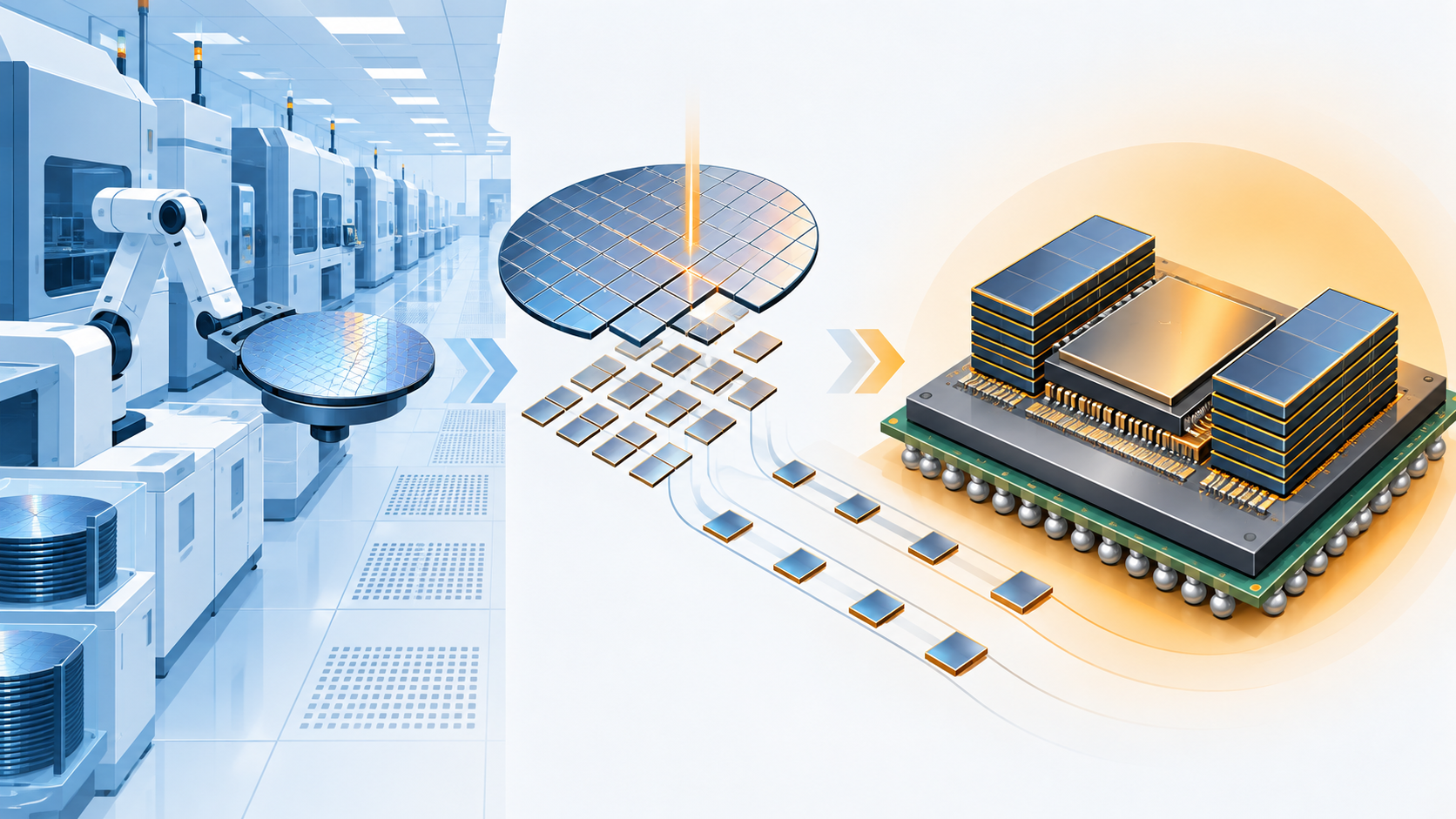 AI-generated concept
13. References
- TSMC Form 20-F for the fiscal year ended December 31, 2025 (filed with the U.S. SEC on 16 April 2026). Revenue, headcount, capital expenditure, R&D expense, fab list, customer concentration, revenue by platform, by node and by region, the ownership structure of the subsidiaries JASM, ESMC and TSMC Arizona, risk factors and the land lease exhibit list. https://www.sec.gov/Archives/edgar/data/1046179/000162828026025362/tsm-20251231.htm
- TSMC Fourth quarter 2025 earnings release (Form 6-K, Exhibit 99.1, 15 January 2026). The 2026 capital budget of US$52bn to US$56bn, the 2025 counts of customers, products and process technologies, and quarterly results. https://www.sec.gov/Archives/edgar/data/1046179/000104617926000008/a4q25e_withguidancexfinal.htm
- TSMC December 2025 Revenue Report (Form 6-K, 9 January 2026). Full-year 2025 revenue of NT$3,809,054m, up 31.6% year on year, and the registered office address. https://www.sec.gov/Archives/edgar/data/1046179/000104617926000005/tsm-revenue20260109.htm
- TSMC "TSMC Intends to Expand Its Investment in the United States to US$165 Billion to Power the Future of AI" (Form 6-K, 3 March 2025). The US$165bn U.S. investment, three new fabs, two advanced packaging facilities and an R&D centre, and the naming of Apple, NVIDIA, AMD, Broadcom and Qualcomm as customers. https://www.sec.gov/Archives/edgar/data/1046179/000104617925000024/tsmcexpandinvestmentintheu.htm
- U.S. SEC EDGAR XBRL company facts API (CIK 0001046179). Revenue, capital expenditure and R&D expense for 2021 to 2024, as tagged in each year's Form 20-F. https://data.sec.gov/api/xbrl/companyfacts/CIK0001046179.json
- TSMC Official website, used to check the corporate profile and the brand wordmark. https://www.tsmc.com/english
14. Claim-to-source audit
| Claim in the article | Category | Source |
|---|---|---|
| Legal name, head office address, year founded (1987), listing venues | Sourced | References 1, 3 and 2 https://www.sec.gov/Archives/edgar/data/1046179/000162828026025362/tsm-20251231.htm |
| 2025 revenue of NT$3,809.1bn / US$121.4bn, up 31.6% | Sourced | References 3 and 1 https://www.sec.gov/Archives/edgar/data/1046179/000104617926000005/tsm-revenue20260109.htm |
| Revenue, capex and R&D expense for 2021 to 2024 | Sourced | Reference 5, from each year's Form 20-F https://data.sec.gov/api/xbrl/companyfacts/CIK0001046179.json |
| 2025 R&D expense of about NT$246.4bn | Our calculation | Derived from the "+NT$42,245m year on year" in reference 1 and the 2024 actual in reference 5 https://www.sec.gov/Archives/edgar/data/1046179/000162828026025362/tsm-20251231.htm |
| 90,557 employees, with the splits by function, region and education | Sourced | Reference 1 https://www.sec.gov/Archives/edgar/data/1046179/000162828026025362/tsm-20251231.htm |
| 78,207 employees in Taiwan, 86% of the total | Our calculation | Sum of the seven Taiwan locations in the regional table of reference 1 https://www.sec.gov/Archives/edgar/data/1046179/000162828026025362/tsm-20251231.htm |
| Wafer manufacturing at 85.9% of revenue and non-wafer at NT$536.5bn | Our calculation | The node-by-node revenue total of NT$3,272.6bn in reference 1 against total revenue. The company states only "about 86%" https://www.sec.gov/Archives/edgar/data/1046179/000162828026025362/tsm-20251231.htm |
| 2025 revenue by platform, including HPC at 58% | Sourced | Reference 1 https://www.sec.gov/Archives/edgar/data/1046179/000162828026025362/tsm-20251231.htm |
| Customer concentration: top ten 78%, largest 19%, second 17% | Sourced | Reference 1 https://www.sec.gov/Archives/edgar/data/1046179/000162828026025362/tsm-20251231.htm |
| Fab locations, start years and leading nodes; the AP7 and AP8 land leases | Sourced | Reference 1 https://www.sec.gov/Archives/edgar/data/1046179/000162828026025362/tsm-20251231.htm |
| 2026 capital budget of US$52bn to US$56bn | Sourced | References 2 and 1 https://www.sec.gov/Archives/edgar/data/1046179/000104617926000008/a4q25e_withguidancexfinal.htm |
| US$165bn of U.S. investment including two advanced packaging facilities | Sourced | Reference 4 https://www.sec.gov/Archives/edgar/data/1046179/000104617925000024/tsmcexpandinvestmentintheu.htm |
| CHIPS Act direct funding of US$6.6bn and loans of US$5bn; EUR 5bn in Germany | Sourced | Reference 1 https://www.sec.gov/Archives/edgar/data/1046179/000162828026025362/tsm-20251231.htm |
| Ownership of JASM (Sony, DENSO, Toyota) and ESMC (Bosch, Infineon, NXP) | Sourced | Reference 1 https://www.sec.gov/Archives/edgar/data/1046179/000162828026025362/tsm-20251231.htm |
| Apple, NVIDIA, AMD, Broadcom and Qualcomm named as customers | Sourced | Reference 4, TSMC's own release https://www.sec.gov/Archives/edgar/data/1046179/000104617925000024/tsmcexpandinvestmentintheu.htm |
| 2nm volume production in 2025 and 16A risk production due in 2026 | Sourced | Reference 1 https://www.sec.gov/Archives/edgar/data/1046179/000162828026025362/tsm-20251231.htm |
| Capex at 33.4% of revenue; the 4.5% revenue decline in 2023 | Our calculation | Derived from the figures in references 1 and 5 https://www.sec.gov/Archives/edgar/data/1046179/000162828026025362/tsm-20251231.htm |
| CoWoS world share and capacity in wafers per month | Not yet confirmed | No primary source exists, so this article states no figure |
| TSMC back-end revenue on its own | Not yet confirmed | Not disclosed. Our calculation gives only the ceiling of NT$536.5bn |
| Construction timing and scale of the U.S. advanced packaging facilities | Not yet confirmed | Reference 4 records only that the plan exists; no details are published https://www.sec.gov/Archives/edgar/data/1046179/000104617925000024/tsmcexpandinvestmentintheu.htm |
| Trading relationships with Ajinomoto, Ibiden, Unimicron, ASMPT and others | Not yet confirmed | Absent from TSMC's own primary material, so this article does not treat them as partnerships |
| The outlook in section 10 | Not yet confirmed | An interpretation by this article, drawn from the six items in the facts table |
Last updated 21 September 2026 / Troy Technical
Every figure in this article comes from TSMC's statutory filings with the U.S. Securities and Exchange Commission or from the company's own announcements. No research-firm estimates or press-based figures have been used.