TECHNOLOGY EXPLAINER
What CoWoS Is
— the TSMC packaging technology that gates the supply of AI silicon
When people say that AI chips are supply-constrained, the constraint they are usually describing is this one technology. Its name is nothing more than the order of the assembly steps, written out. What sits behind that plain name is an attempt to push past the physical limit of the lithography scanner using packaging rather than lithography. Written to be readable both by newcomers and by engineers who work with materials.
- What CoWoS is — the name is the process
- Why it is needed
- Three variants: CoWoS-S, -R and -L
- How the reticle limit was beaten — mask stitching
- How big does it get (the roadmap)
- A materials engineer's view: large-area silicon is an awkward object
- Where it sits among TSMC's "three pillars"
- What is still hard
- Glossary / Primary sources / Claim-to-source audit
Sourced = a value stated in published material from a research institute or manufacturer (link given)
Our calculation = a figure this article derived, with the assumptions spelled out
Not yet confirmed = research-stage work with no confirmed production record
1. What CoWoS is — the name is the process
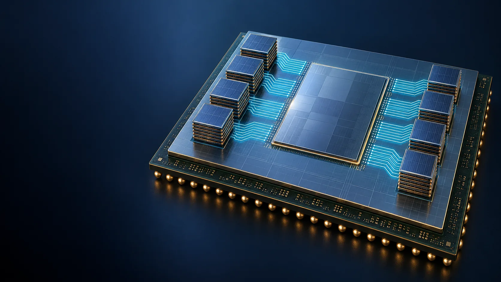
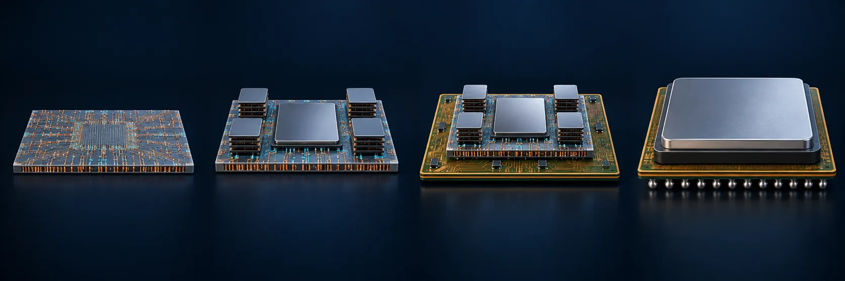
CoWoS stands for Chip on Wafer on Substrate. It looks like jargon, but the name is simply the assembly sequence written out in order.
- Chip on Wafer: the chips — logic dies and HBM stacks — go onto a wafer first. That wafer is the interposer.
- on Substrate: the piece is then cut out of that wafer and mounted on the package substrate.
TSMC describes CoWoS as a 2.5D advanced packaging technology that integrates multiple SoCs and high bandwidth memory (HBM) stacks to deliver high computing performance and memory bandwidth in a productSourced (TSMC).
2. Why it is needed
Several threads from earlier articles in this series come together here.
| The requirement | What CoWoS does about it |
|---|---|
| Put HBM next to the processor | High bandwidth memory only performs if it sits a few millimetres from the processor. The interposer is the platform that makes those few millimetres possible |
| Connect chiplets to each other | Links the split dies with dense wiring on a micrometre pitch |
| Get past the reticle limit | Builds a system larger than any single die could be, by placing several dies side by side |
TSMC states that the CoWoS platform has kept evolving since volume production began in 2012, and that the arrival of generative AI in the second half of 2022 pushed market demand higher stillSourced.
Building an AI accelerator takes logic dies and HBM, but without the step that joins them into one part there is no product. That step needs a silicon interposer — a component made on a semiconductor process line — plus dedicated assembly equipment. This is why it is possible to have plenty of front-end wafer capacity and still no finished product.
3. Three variants: CoWoS-S, -R and -L
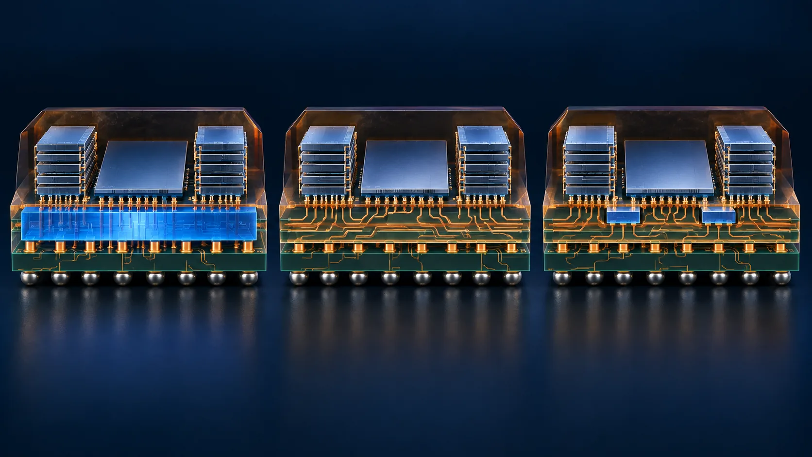
CoWoS comes in three variants, and what separates them is what the chips are connected through.
| Variant | What connects the chips | How TSMC describes it |
|---|---|---|
| CoWoS-S | Silicon interposer | A large-area silicon interposer carrying dense wiring and an embedded deep trench capacitor (eDTC), with logic chiplets and other dies mounted on it and HBM stacked above. In production since 2012, with the interposer going up to 3.3 reticles |
| CoWoS-R | RDL interposer | An RDL interposer is used for the interconnect between SoCs and HBM. In volume production since 2023. The RDL interposer is made of polymer and copper wiring and is relatively flexible, which improves the integrity of the C4 joints and allows larger packages to meet more complex functional requirements |
| CoWoS-L | RDL plus embedded silicon bridges | Combines Chip on Wafer on Substrate with an RDL-based interposer, a denser embedded local silicon interconnect (LSI), eDTC and the integration of various embedded chips, enabling larger HPC products |
All of the above is Sourced (TSMC CoWoS technology page). TSMC recommends CoWoS-L or CoWoS-R for sizes beyond 3.3 reticles.
As you move from S to R to L, the design steps further away from being all silicon. Silicon gives the finest wiring, but it is stiff, brittle and expensive per unit area. So the larger the package has to be, the more the design confines silicon to the places that actually need it — and CoWoS-L, which buries a silicon bridge only where the dense links are, is where that logic ends up.
4. How the reticle limit was beaten — mask stitching
This, to my mind, is the most interesting part of the whole technology.
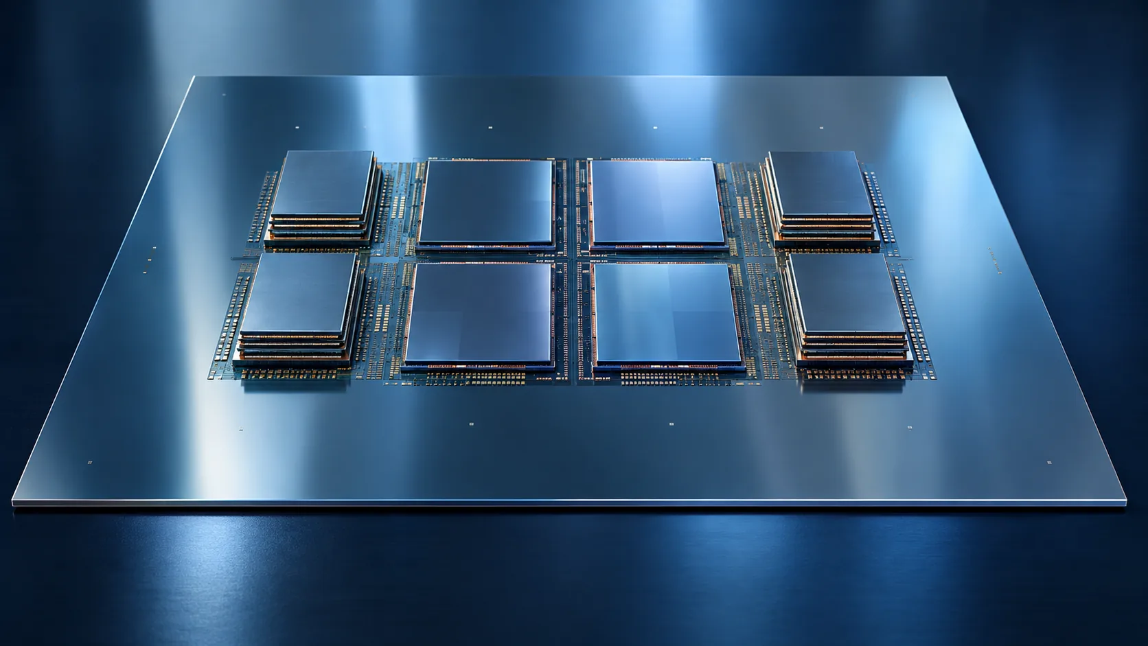
As the article on chiplets explained, there is an upper bound on the area a lithography scanner can print in a single exposure: the reticle limit. TSMC puts one reticle at roughly 830 mm²Sourced.
Yet an interposer has to carry a logic die and several HBM stacks side by side. There is no way that fits inside 830 mm².
The answer: stitch the exposures together
On 3 March 2020, TSMC announced, in collaboration with Broadcom, the industry's first and largest 2x reticle size interposer, about 1,700 mm² in areaSourced.
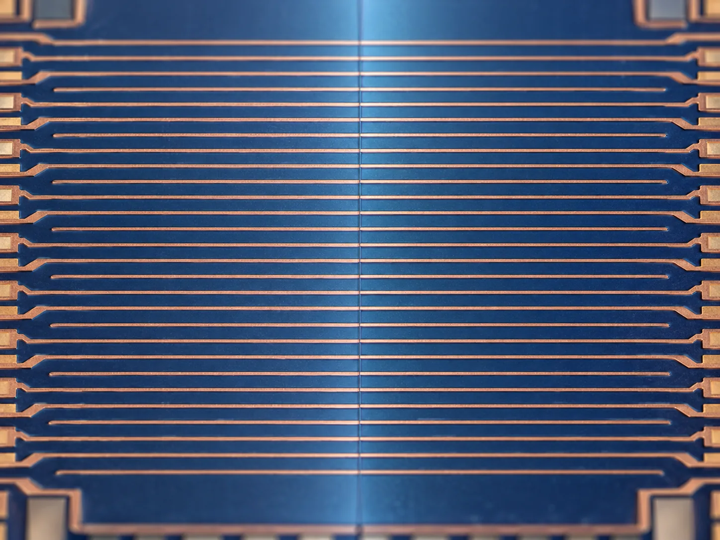
What made it possible was TSMC's unique mask stitching process that allows the interposer to extend beyond full reticle sizeSourced (TSMC, 3 March 2020).
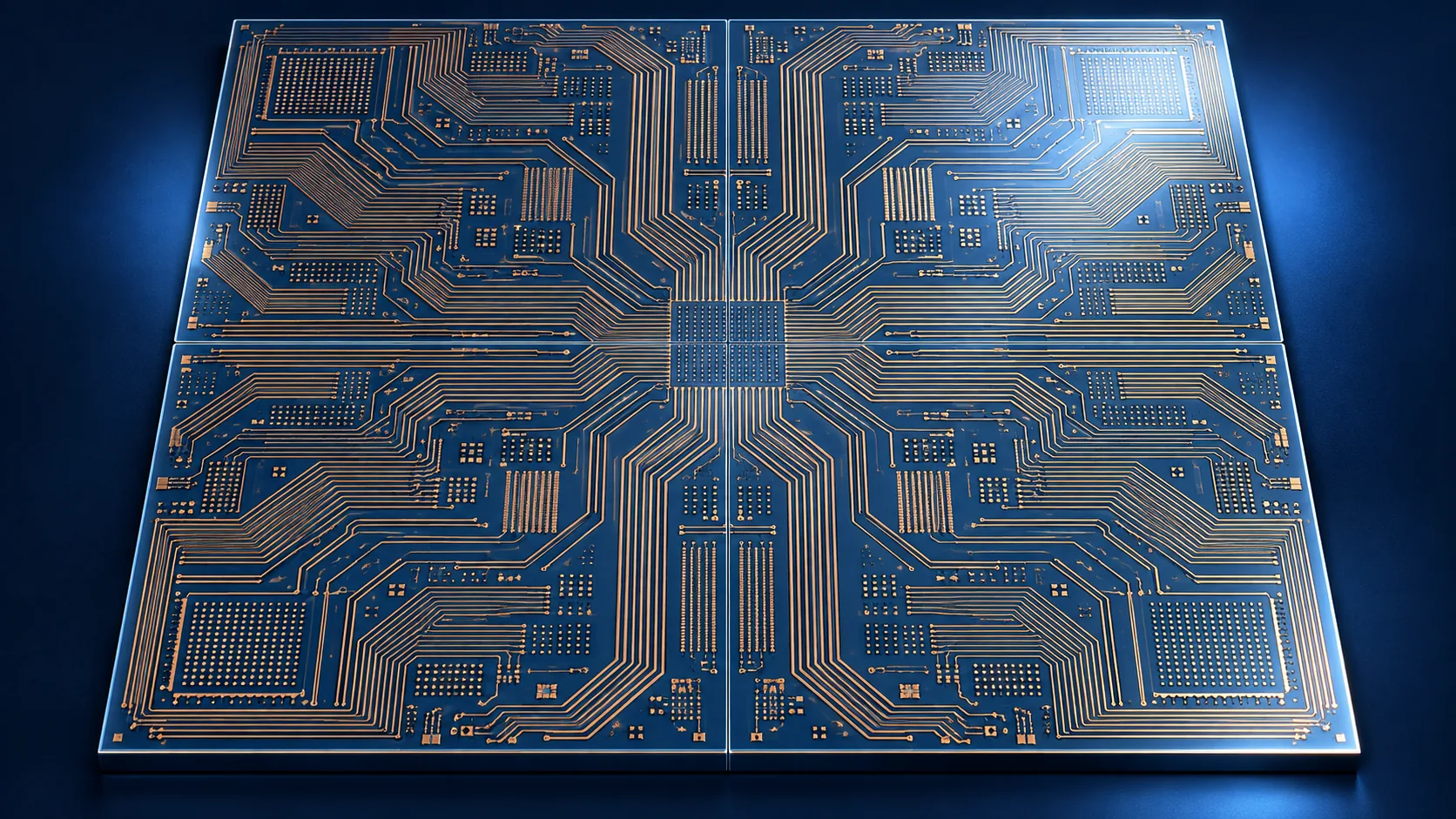
The configuration that resulted was published too: multiple logic SoC dies together with up to six HBM cubes, up to 96 GB in total, and up to 2.7 TB/s of bandwidth. That is 2.7 times the CoWoS offering of 2016Sourced.
Who did what was stated as well: Broadcom defined the complex configuration of the top dies, interposer and HBM, while TSMC developed the robust manufacturing process that maximises yield and performanceSourced.
5. How big does it get (the roadmap)
TSMC has published its plans for scaling CoWoS up, one technology symposium at a time.
| Generation | Area (calculated) | Share of a 300 mm wafer | Source and date |
|---|---|---|---|
| 2 reticles | approx. 1,700 mm² | approx. 2.4% | Published by TSMC (March 2020) |
| 3.3 reticles | approx. 2,700 mm² | approx. 3.8% | TSMC CoWoS technology page |
| 5.5 reticles | approx. 4,600 mm² | approx. 6.5% | "In production", published by TSMC (April 2026) |
| 9.5 reticles | approx. 7,900 mm² | approx. 11% | Volume production planned for 2027 (April 2025) |
| 14 reticles | approx. 11,600 mm² | approx. 16% | Planned for 2028 (April 2026) |
| 40 reticles (SoW-X) | approx. 33,200 mm² | approx. 47% | Expected 2029 (April 2026) |
The reticle counts and dates are Sourced (published by TSMC). The areas and percentages are Our calculation, taking one reticle as 830 mm² and a 300 mm wafer as π × 150² = approx. 70,686 mm². TSMC publishes the areas for the 2-reticle and 3.3-reticle cases directly.
Fourteen reticles works out to roughly a 108 mm square of siliconOur calculation. A single product would then occupy about one sixth of a whole 300 mm wafer.
In its April 2025 announcement TSMC put volume production of SoW-X in 2027; in its April 2026 announcement the 40-reticle SoW-X is listed as expected in 2029Sourced. The two share a product name but are not quoting the same metric, so this cannot simply be read as a delay. We mention it as an illustration that roadmap numbers get revised, and should always be quoted with the date they were announced.
6. A materials engineer's view: large-area silicon is an awkward object
Looked at from the materials side, CoWoS is the art of handling a piece of silicon that has no business being that large, without breaking it.
(1) A huge piece of silicon, thinned and bonded
A 3.3-reticle interposer is about 2,700 mm², which is a 52 mm square of siliconOur calculation. On top of that, the interposer has to be thinned so that TSVs can run right through it. Large, thin, stiff and brittle — every condition for warpage and cracking is present at once.
(2) The CTE mismatch scales with the dimension
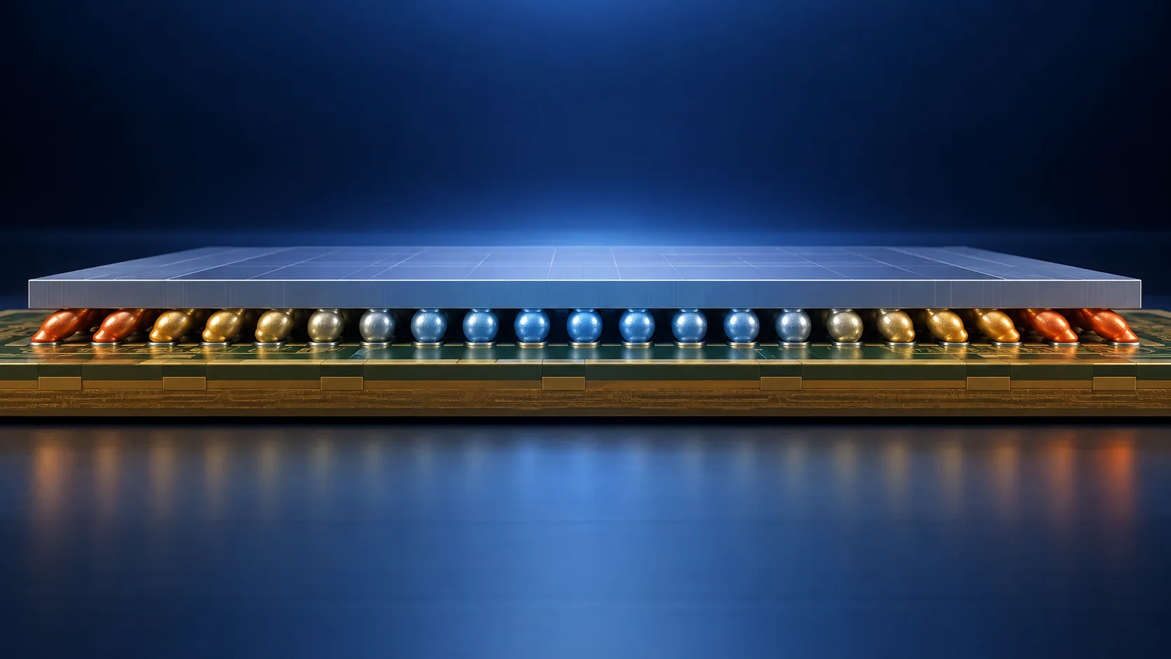
Inside the package sit three layers with different thermal expansion: the silicon interposer (expands little), the C4 bumps, and the organic package substrate (expands a lot).
Change the temperature and the three grow and shrink by different amounts — and the difference grows in proportion to the distance from the centre. On a 52 mm square the displacement mismatch at the edge is moderate; at 108 mm square it is, to first order, twice as large. Every step up in size adds a linear increase in the load carried by the outermost bumps.
When TSMC says of CoWoS-R that the RDL interposer is relatively flexible, which improves the integrity of the C4 joints and enables larger packages, it is answering exactly this problemSourced. Swapping a stiff material for a compliant one was what broke the size barrier — a case where a mechanical property, not an electrical one, decided the technology choice.
(3) Accuracy at the seam
Mask stitching requires the wiring to join up across the boundary between adjacent exposure fields. The overlay accuracy achieved there translates directly into wiring yield. The larger the interposer, the more seams there are; and because the area is large, temperature drift during exposure and wafer warpage show up as misregistration all the more readily.
(4) Building function into the interposer
For CoWoS-S and CoWoS-L, TSMC lists an eDTC, an embedded deep trench capacitorSourced. Deep trenches are etched into the silicon, then lined with a dielectric and electrodes to form a capacitor.
So the interposer is not merely a wiring board; it is somewhere you can build the parts that damp power-supply noise. Depositing a uniform film all the way down a deep trench is a demanding piece of process technology, and its presence here shows how far front-end materials and process technology have moved into packaging.
7. Where it sits among TSMC's "three pillars"
TSMC organises its chip-to-chip interconnect technologies into three pillarsSourced (TSMC Research).
| Pillar | How it connects | The technology | Article in this series |
|---|---|---|---|
| Silicon interposer | Fine wiring on silicon | CoWoS | This article |
| High-density, fine-pitch fan-out RDL | Redistribution layers on polymer | InFO | The RDL article |
| Bumpless bonding | Copper bonded directly to copper | SoIC | The hybrid bonding article |
TSMC lists the strengths of the silicon interposer as high wiring density, high capacitance per unit area, and a large reticle size for exascale HPC and AISourced. The fact that "large reticle size" is listed as a strength alongside the performance metrics tells you a great deal about the character of this technology.
8. What is still hard
(1) Capacity
CoWoS needs an interposer built on a silicon process line, just like front-end manufacturing, plus dedicated assembly equipment. Adding equipment takes time, so capacity cannot follow a demand spike quickly. TSMC itself says demand grew further with the arrival of generative AISourced.
(2) Size versus yield
The more area a part occupies, the higher the chance it contains a defect. And by that point the interposer is already carrying expensive dies that have been tested and confirmed good. A failure at the final assembly stage throws away everything invested up to that point.
(3) Heat
Ten logic dies and twenty HBM stacks in a single package: if the 2028 plan is realised, getting the resulting heat out becomes the next wall. TSMC's research publications include work on liquid cooling for HPCSourced.
9. Glossary
- CoWoS
- Chip on Wafer on Substrate. TSMC's 2.5D advanced packaging technology.
- 2.5D packaging
- Laying several dies out on a plane and connecting them densely through a shared platform. Distinct from 3D, where dies are stacked vertically.
- Interposer
- The intermediate board that carries the dies and interconnects them. Made either of silicon or of RDL.
- Reticle
- The area a scanner can print in one exposure. TSMC puts one reticle at about 830 mm².
- Mask stitching
- Joining adjacent exposure fields together to build an area larger than the reticle limit.
- CoWoS-S
- The variant using a silicon interposer. The densest of the three, up to 3.3 reticles.
- CoWoS-R
- The variant using an RDL interposer. Its compliance improves C4 joint reliability.
- CoWoS-L
- The variant combining RDL with embedded silicon bridges (LSI).
- LSI
- Local Silicon Interconnect. A piece of silicon interconnect embedded only where it is needed.
- eDTC
- Embedded deep trench capacitor. A capacitor formed in deep trenches etched into silicon, used to damp power-supply noise.
- C4 bump
- The solder bump connecting the interposer to the package substrate.
- SoW-X
- A wafer-scale system integration technology built on CoWoS, at the 40-reticle scale.
- TSV
- Through-Silicon Via. Connects the front and back of the interposer.
10. Primary sources
- TSMC "CoWoS®" technology page — 3dfabric.tsmc.com
- TSMC "TSMC and Broadcom Enhance the CoWoS Platform with World's First 2X Reticle Size Interposer", 3 March 2020 — pr.tsmc.com
- TSMC "TSMC Unveils Next-Generation A14 Process at North America Technology Symposium", 23 April 2025 — pr.tsmc.com
- TSMC "TSMC Debuts A13 Technology at 2026 North America Technology Symposium", April 2026 — pr.tsmc.com
- TSMC Research "Interconnect / Off-chip Interconnect" — research.tsmc.com
- TSMC "TSMC-SoIC®" technology page — 3dfabric.tsmc.com
11. Claim-to-source audit
| Claim in the text | Basis | Label |
|---|---|---|
| CoWoS is a 2.5D advanced packaging technology that integrates multiple SoCs and HBM stacks to deliver high computing performance and memory bandwidth. Volume production began in 2012, and demand grew further with the arrival of generative AI in the second half of 2022 | TSMC CoWoS technology page[Source 1] https://3dfabric.tsmc.com/english/dedicatedFoundry/technology/cowos.htm | Sourced |
| CoWoS-S goes up to 3.3 reticles (approx. 2,700 mm²). Beyond 3.3 reticles TSMC recommends CoWoS-L or CoWoS-R | TSMC CoWoS technology page[Source 1] https://3dfabric.tsmc.com/english/dedicatedFoundry/technology/cowos.htm | Sourced |
| CoWoS-S carries dense wiring and an embedded deep trench capacitor on a silicon interposer, with HBM stacked above. In production since 2012 | TSMC CoWoS technology page[Source 1] https://3dfabric.tsmc.com/english/dedicatedFoundry/technology/cowos.htm | Sourced |
| CoWoS-R uses an RDL interposer and has been in volume production since 2023. The RDL interposer is made of polymer and copper wiring, is relatively flexible, improves C4 joint integrity and enables larger packages | TSMC CoWoS technology page[Source 1] https://3dfabric.tsmc.com/english/dedicatedFoundry/technology/cowos.htm | Sourced |
| CoWoS-L combines an RDL-based interposer, a denser embedded LSI, eDTC and various embedded chips | TSMC CoWoS technology page[Source 1] https://3dfabric.tsmc.com/english/dedicatedFoundry/technology/cowos.htm | Sourced |
| One reticle is approximately 830 mm² | TSMC CoWoS technology page[Source 1] https://3dfabric.tsmc.com/english/dedicatedFoundry/technology/cowos.htm | Sourced |
| On 3 March 2020 TSMC and Broadcom announced the industry's first 2x reticle size interposer (approx. 1,700 mm²), extended beyond full reticle size by a unique mask stitching process. Up to six HBM cubes (up to 96 GB), up to 2.7 TB/s of bandwidth, 2.7 times the 2016 offering. Broadcom defined the configuration and TSMC developed the manufacturing process | TSMC press release, 3 March 2020[Source 2] https://pr.tsmc.com/english/news/2026 | Sourced |
| A 9.5-reticle CoWoS is planned for volume production in 2027 and can integrate 12 or more HBM | TSMC press release, 23 April 2025[Source 3] https://pr.tsmc.com/english/news/3228 | Sourced |
| A 5.5-reticle CoWoS is in production. Fourteen reticles (about 10 logic dies plus 20 HBM) is planned for 2028, with more than 14 reticles in 2029. The 40-reticle SoW-X is expected in 2029 | TSMC press release, April 2026[Source 4] https://pr.tsmc.com/english/news/3302 | Sourced |
| The date given for SoW-X differs: 2027 in the 2025 announcement, 2029 in the 2026 announcement | Comparison of two TSMC press releases[Source 3] https://pr.tsmc.com/english/news/3228[Source 4] https://pr.tsmc.com/english/news/3302 | Sourced |
| The area for each reticle count (4,600 / 7,900 / 11,600 / 33,200 mm² and so on), the share of a 300 mm wafer, and the conversions to a 52 mm and a 108 mm square | Our calculation from one reticle = 830 mm² and a 300 mm wafer = π × 150². The areas for 2 and 3.3 reticles are TSMC's published values | Our calculation |
| TSMC organises chip-to-chip interconnect into three pillars (silicon interposer / fan-out RDL / bumpless bonding, that is CoWoS / InFO / SoIC). The strengths of the silicon interposer are high wiring density, high capacitance density and large reticle size | TSMC Research[Source 5] https://research.tsmc.com/english/research/interconnect/off-chip-interconnect/publish-time-1.html | Sourced |
| That displacement from CTE mismatch grows with distance from the centre; that scaling up adds seams and makes misregistration more likely; that uniform deposition into deep trenches is demanding | Commentary based on general relationships in materials engineering and process technology. No numerical claim is made about any specific product | Commentary |
| The roadmap from 2027 onward | TSMC's own outlook, not a production record | Not yet confirmed |
Last updated 20 September 2026. Sources are limited to TSMC's official announcements and technology pages. All figures are explanatory concept graphics. Visual-overview figures are shown as AI-generated conceptual images, matching the Japanese edition. Vector drawings are retained where they carry quantitative values or precision-critical technical labels. AI-generated images do not depict real equipment, products, facilities, dimensions or exact cross-sections; replaced source SVG overview drawings remain in the HTML but are hidden.