

Key Findings
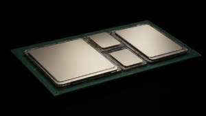
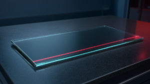
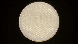
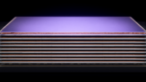
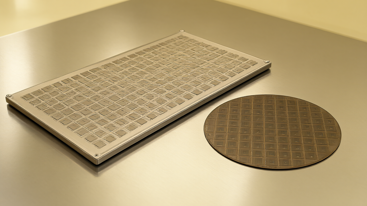
CoPoS is emerging as a successor to CoWoS to address the limitations of traditional wafer-level packaging as GPU and HBM integration scales. According to analysis from Infomarket CEO Yong-woon Kang, TSMC is advancing R&D in this direction, and Samsung Electro-Mechanics is also exploring related technologies. The transition shifts the processing carrier from a circular wafer to a rectangular panel, significantly reducing edge area loss.
Technical Details
The CoPoS workflow utilizes an organic redistribution layer (RDL) as the interposer structure. The process follows these stages:
- RDL Fabrication: Ultra-fine circuits (approximately 2 microns linewidth) are fabricated on a temporary glass carrier.
- Chip Mounting: GPU chips (approx. 26×33mm) and HBM stacks (approx. 11×12mm) are mounted on the RDL with a micro-bump pitch of 25 to 40 microns and alignment accuracy of ±1 to 2 microns.
- Encapsulation: Molding compound encapsulates the chips and RDL for mechanical strength.
- Dicing and Connection: The glass carrier is stripped, and the panel is diced into independent packaged units (69 to 90mm square) before being connected to the organic packaging substrate.
Crucially, the glass in current CoPoS solutions serves as a temporary carrier; the final RDL interposer remains an organic material structure.
Equipment Requirements
The shift to panel sizes expanding from 310×310mm to 515×510mm drives demand for specific hardware:
- 40mm-class TC thermal compression bonders: Used for the initial mounting of GPU and HBM stacks.
- MSVP (Micro SAW & VISION PLACEMENT) systems: Integrated systems for dicing, cleaning, inspection, and placement of the molded panels.
- 120mm-class TC bonders: Used for the final connection between the packaged unit and the substrate.
Significance and Outlook
The transition to CoPoS allows for a processing area more than 3.5 times larger than a 300mm wafer. Future growth in equipment demand is expected to align with the development of glass interposers and glass core substrates.
Source: https://eu.36kr.com/en/p/4042012488962946
Get our weekly technology intelligence — free
Receive an infographic that lets you judge at a glance whether each field’s analysis report is worth reading.
Subscribe Free — Weekly Tech Intelligence
By subscribing, you’ll receive Troy-Technical’s weekly technology intelligence newsletter.
- Your email and selected fields are used only to deliver the newsletter.
- We never share your information with third parties.
- You can unsubscribe anytime via the link in each email.
See our Privacy Policy for details.
Takes about a minute · Unsubscribe anytime