TECHNOLOGY EXPLAINER
What an Interposer Is
— silicon, organic, glass: the platform material sets the ceiling
An interposer is the intermediate board that sits between the dies and the package substrate. What it is made of decides how large a package you can build, how fine the wiring can be, and how reliable the result is. This article compares the material systems side by side.
- What an interposer is (the short version)
- Why you need one — two jobs
- Four material systems
- Silicon interposers
- RDL (organic) interposers
- Glass interposers
- A materials engineer's view: three limits set by the material
- How to choose
- Glossary / Primary sources / Claim-to-source audit
Sourced = a value stated in published material from a manufacturer or research institute (link given)
Our calculation = a figure this article derived, with the assumptions spelled out
Not yet confirmed = a plan or target with no confirmed production record
1. What an interposer is (the short version)
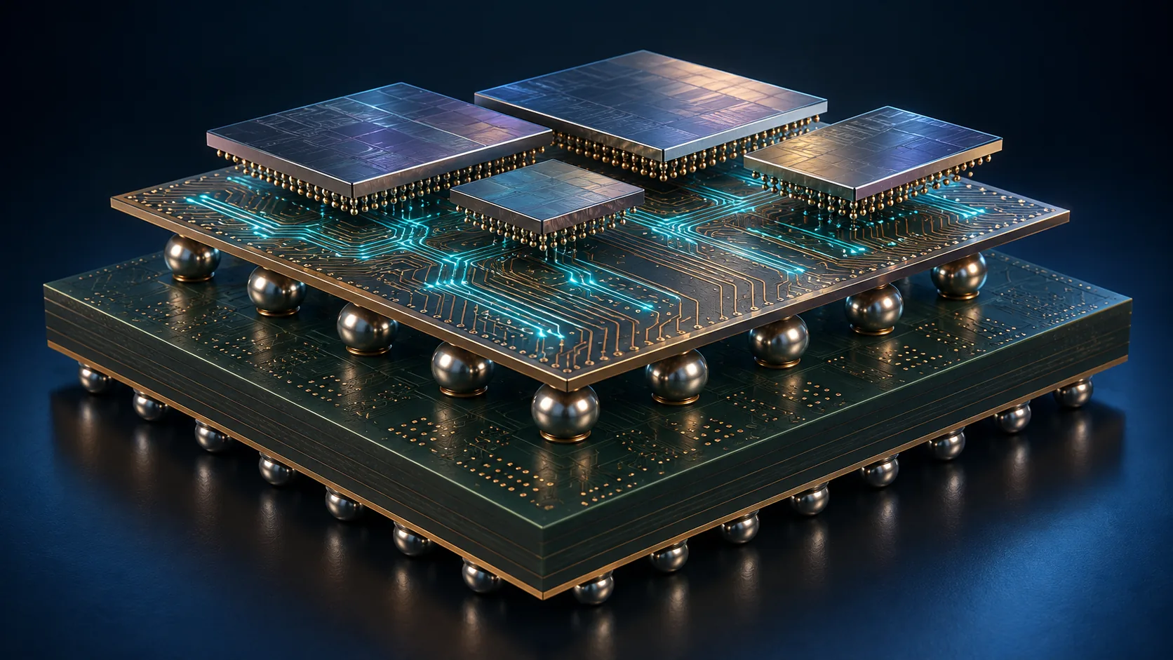
An interposer is an intermediate wiring board placed between the dies and the package substrate. The name is literal: it is interposed between the two.
- It carries: several dies side by side (a compute die, HBM stacks and so on)
- It links: those dies to each other with micrometre-scale wiring
- It hands down: the signals, converted to terminals coarse enough for the substrate below to handle
The Package Substrate article described the substrate as a converter between the nanometre and the millimetre. An interposer is one more step inserted into that conversion. Die terminals became too fine to reach the substrate directly, so an intermediate step was needed. That framing makes the rest straightforward.
2. Why you need one — two jobs
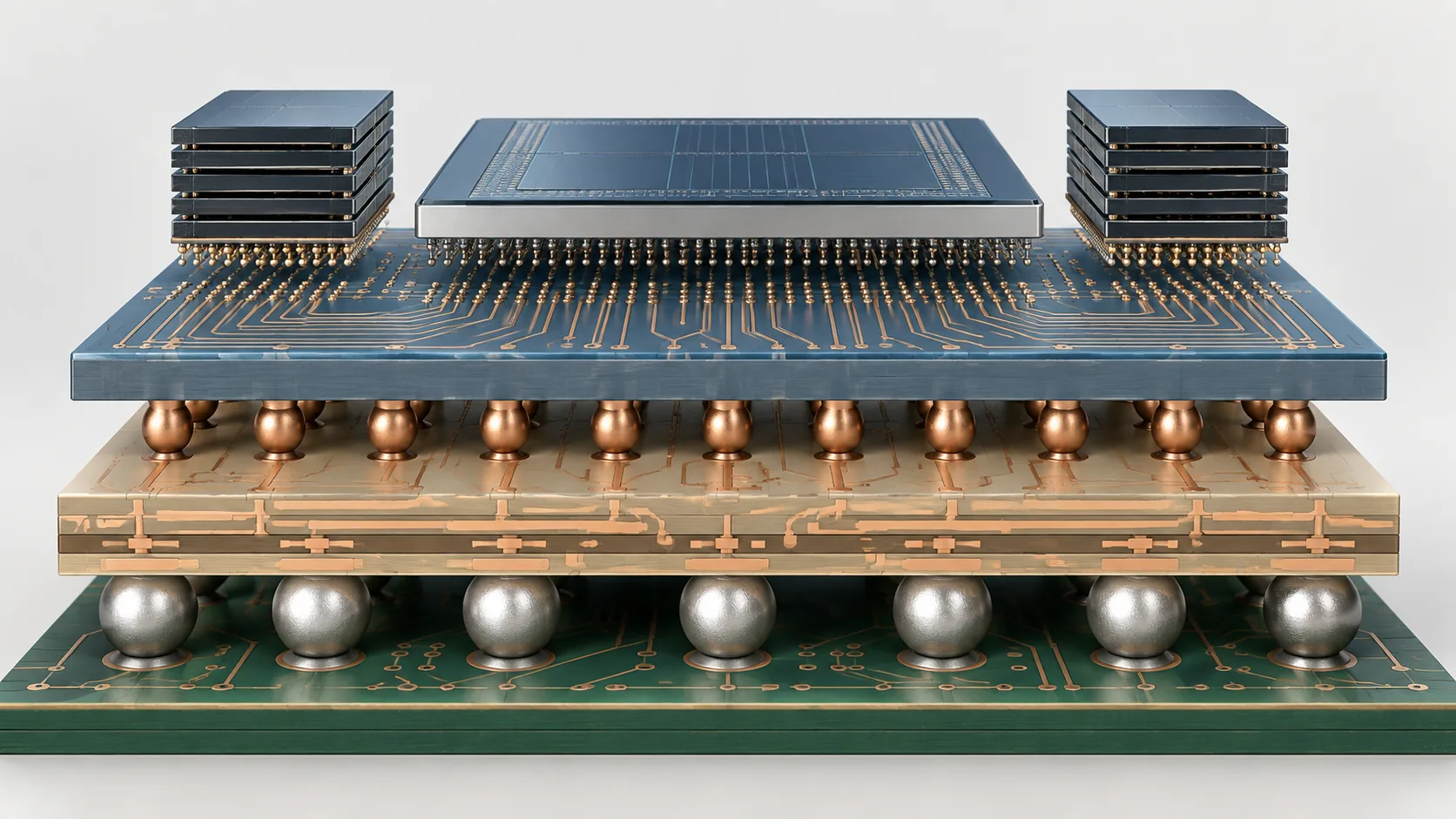
Job 1: link dies to each other more finely than the substrate can
Mounting chiplets or HBM requires very fine wiring between the dies. Package substrate wiring cannot be made that fine. So you lay a board capable of wiring at least an order of magnitude finer than the substrate directly under the dies.
Job 2: convert terminal pitch
Terminals on the underside of a die are extremely fine; the substrate cannot receive them. The interposer takes them, fans them out, and passes them down.
Every additional part means more process steps, more cost and more reliability risk. If the substrate could make fine enough wiring, you would not want an interposer at all. Seen that way, the bridge approach — embedding a small piece of silicon only where it is needed — and the UHDI push to make substrates themselves finer both read as attempts to make the interposer thinner, smaller, or unnecessary.
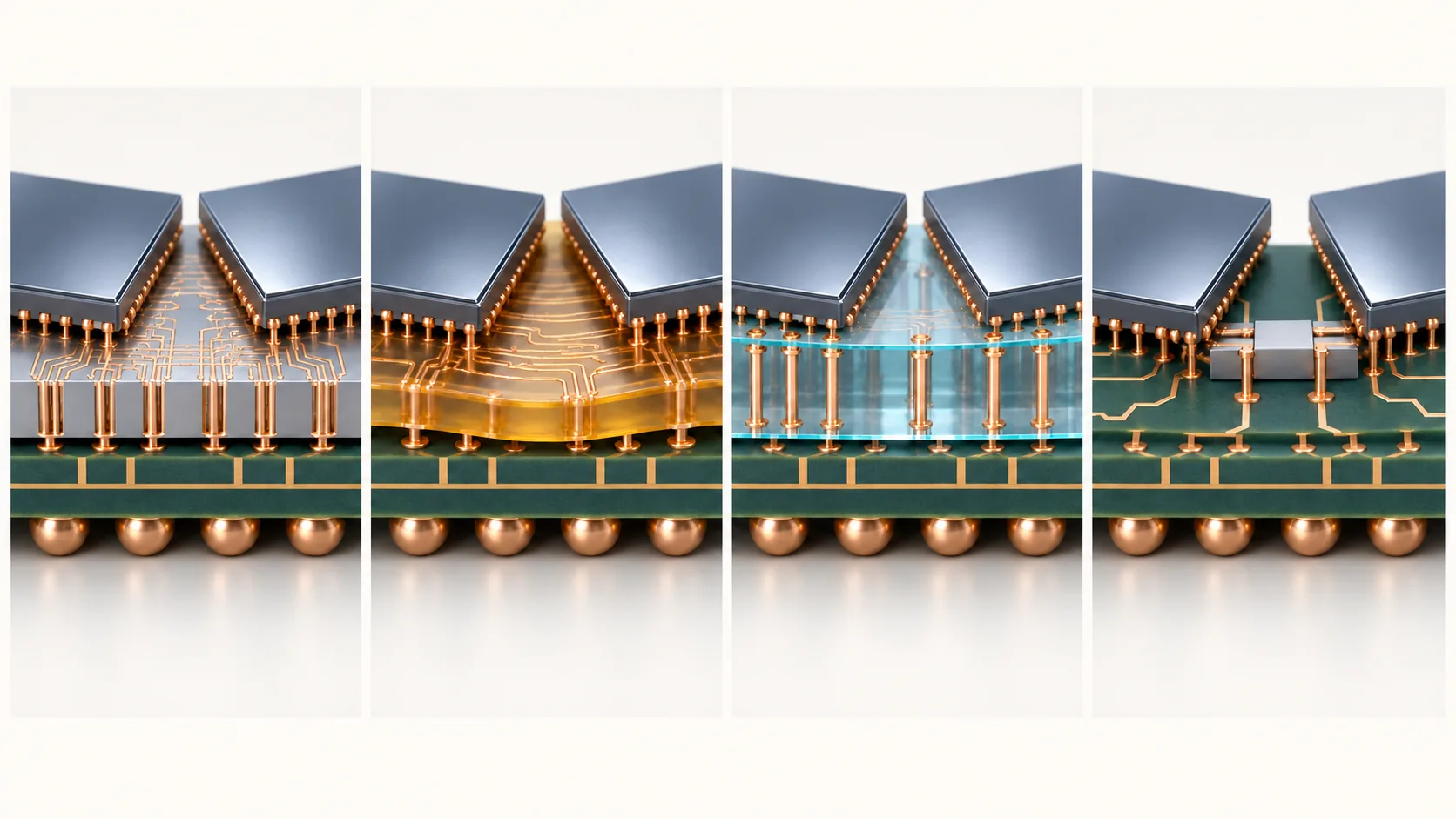
3. Four material systems
An interposer's character depends almost entirely on what it is made of. That is the subject of this article.
4. Silicon interposers
The oldest approach, and the one that supports the finest wiring.
TSMC describes CoWoS-S as placing high-density interconnect and embedded deep trench capacitors on a large silicon interposer, mounting logic chiplets and stacking HBM on topSourced. It has been in production since 2012, with interposer size up to 3.3 reticles (about 2,700 mm squared)Sourced (TSMC).
How fine does it get? imec's published figures
On 27 May 2025 imec published concrete numbers for its 300 mm RF silicon interposer platformSourced (imec).
| Item | Published value |
|---|---|
| Insertion loss | 0.73 dB/mm up to 325 GHz, described as a record low |
| RF and microwave transmission lines | 5 µm line width, 5 µm spacing |
| Digital interconnect | Line and space of 1 µm / 1 µm |
| Flip-chip pitch | 40 µm, with work under way toward 20 µm |
| What can be integrated | Digital, analogue, RF to sub-THz CMOS and III-V chiplets on a single carrier |
| Planned additions | TSVs, a backside redistribution layer, and MIMCAP for power decoupling |
All rows Sourced (imec, 27 May 2025). These are research platform values and do not represent production-level capability.
It is easy to assume a silicon interposer must have TSVs, but on this imec platform TSVs are listed as a future additionSourced.
In other words, an interposer does not require TSVs by definition. If the job is only to link dies laterally, surface wiring layers are enough. TSVs become necessary only once signals have to pass vertically down to the package substrate. The structure you need follows from the job you assign it.
As a follow-up: the MIMCAP listed as a future addition in May 2025 was reported in imec's June 2026 announcement as reaching 10 to 100 times the capacitance density of typical on-chip capacitors in III-V technologySourced (covered in the Heterogeneous Integration article).
5. RDL (organic) interposers
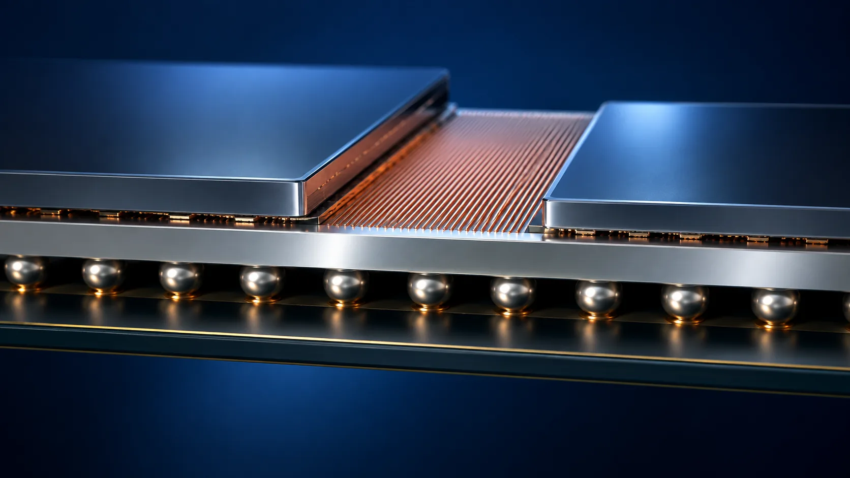
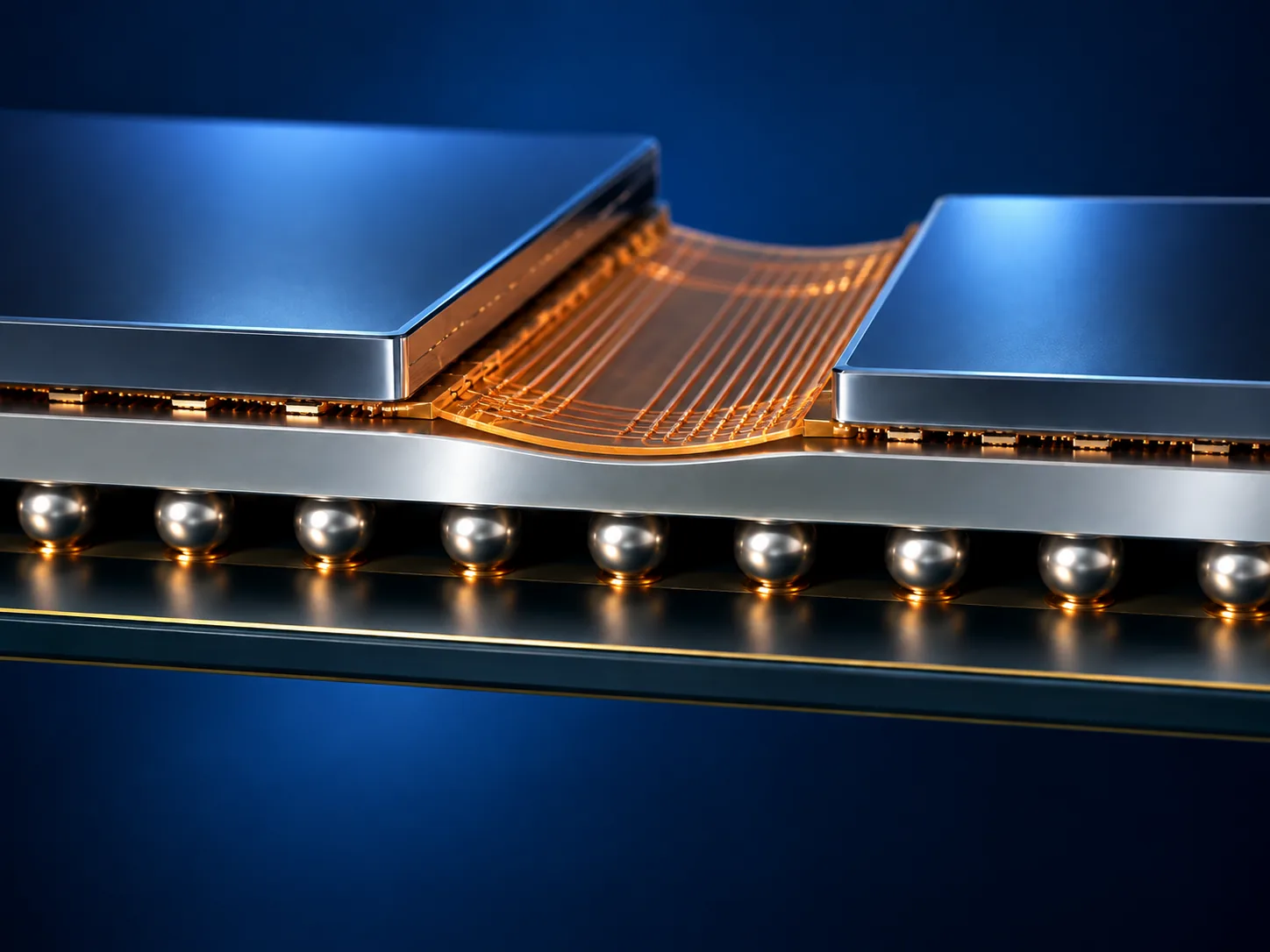
Instead of silicon, this approach builds the interposer from polymer and copper wiring layers.
TSMC describes CoWoS-R as using an RDL interposer for the interconnect linking SoC and HBM, in volume production since 2023Sourced, and characterises it as follows.
"The RDL interposer, which consists of polymer and copper trace, is relatively flexible. This enhances the C4 joint integrity and enables package size expansion to accommodate extremely complicated functional requirements." (TSMC)
TSMC recommends CoWoS-L or CoWoS-R for sizes beyond 3.3 reticlesSourced. In other words, when the package gets large, the organic route is chosen over silicon.
Building them on panels
On 3 September 2025 Resonac launched JOINT3, a consortium of 27 companies, to develop the manufacturing process for panel-level organic interposers at 515 x 510 mmSourced. The pilot line is scheduled to run in 2026 (Resonac).
A silicon interposer is bound to the round wafer and the reticle; an organic interposer can be built on a large rectangular panel. The area-efficiency argument from the PLP article applies here directly.
6. Glass interposers
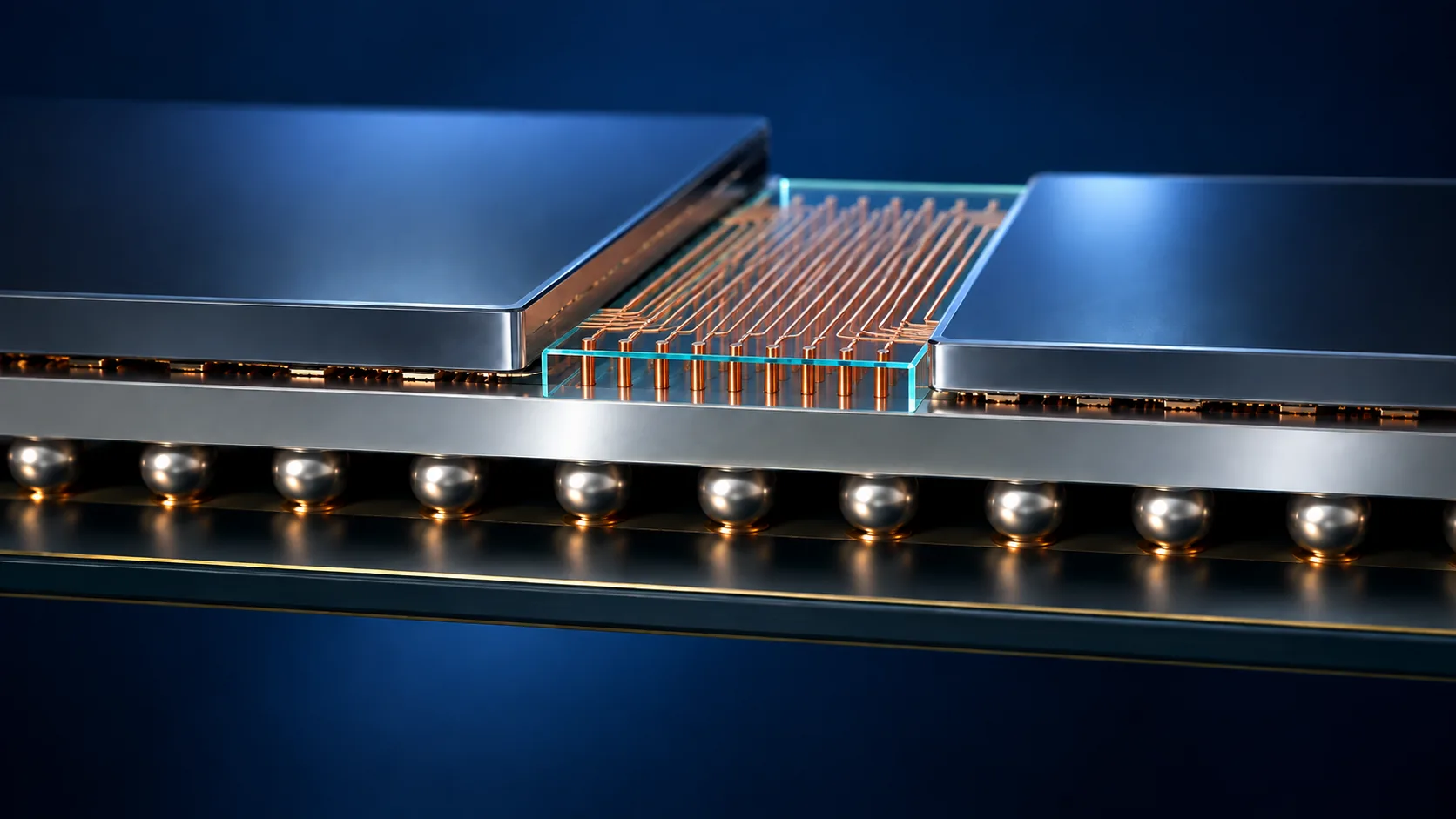
The third option is glass. The material covered in the Glass Substrate article is being considered not only as a core substrate but as an interposer.
AT&S lists the advantages of glass as a coefficient of thermal expansion that can be designed close to silicon, extremely low TTV (total thickness variation) and low warpage, high resistivity and low loss tangent, and — unlike a silicon interposer — the ability to be formed in large panelsSourced (AT&S).
AGC states that its thin glass substrates cover thicknesses from 0.1 to over 1.1 mm, can form fine TGVs of 50 µm diameter and above at tight pitch, and support high aspect ratios (up to 20:1 at 1.0 mm thickness), with applications in 3D packaging, chiplets, CPO substrates and RF devicesSourced (AGC).
As stated in the Glass Substrate article, as of our research date (September 2026) we could not find an official announcement from any manufacturer declaring the start of volume production of glass core substrates or glass interposersNot yet confirmed. Published targets sit in 2027 to 2028 and beyond.
7. A materials engineer's view: three limits set by the material
Line the four approaches up and it becomes clear that almost all the performance differences follow from material properties.
| Limit | Silicon | RDL (organic) | Glass |
|---|---|---|---|
| 1. Size | Up to 3.3 reticles (about 2,700 mm squared) beyond that, CoWoS-L/R is recommended | Can be built on large panels 515 x 510 mm under development | Can be formed in large panels named as an advantage over silicon |
| 2. Wiring fineness | L/S of 1 µm / 1 µm (published by imec) | Does not reach silicon | Flatness is said to favour fine patterning |
| 3. Mechanical behaviour | Hard and brittle; large sizes load the joints | Flexible, improving C4 joint integrity | Brittle, though low warpage is an advantage |
Compiled from each company's published material. The axes of comparison were chosen by this article and are not a standardised classification.
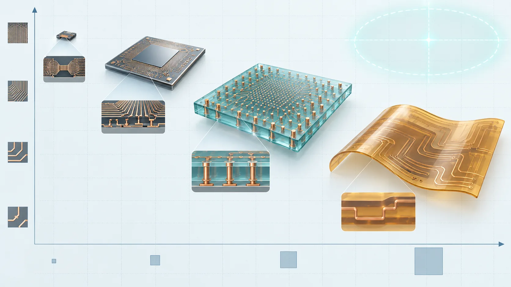
No material has reached the top right — large and fine at the same time. Silicon is fine but cannot be made large. Organic can be made large but concedes on fineness. Glass is the candidate for both, but production is still ahead of it.
And the bridge is a solution that steps outside the map altogether. It gives up on making the whole area high-density and embeds silicon only where it is needed. Intel has published a move from 55 µm to 45 µm bump pitch in its second-generation EMIBSourced, and TSMC combines an RDL interposer with embedded local silicon interconnect (LSI) in CoWoS-LSourced.
If the material cannot do both, split the job structurally — that is the practical answer at this point.
8. How to choose
| Requirement | Likely choice | Basis |
|---|---|---|
| Highest possible die-to-die density | Silicon | L/S of 1 µm / 1 µm has been published |
| Larger than 3.3 reticles | RDL, or RDL plus a bridge | TSMC recommends CoWoS-L/R beyond 3.3 reticles |
| Worried about joint reliability at large sizes | RDL | "Relatively flexible, enhancing C4 joint integrity" (TSMC) |
| Need low loss at high frequency | Silicon designed for low loss, or glass | imec reports 0.73 dB/mm to 325 GHz; AT&S cites glass's low loss tangent |
| Need lower cost per unit area | RDL built on panels | Large panels improve area efficiency (see the PLP article) |
| High density needed only in places | Bridge | Silicon embedded only where required |
Our own summary. Real choices depend on product specification, cost, supply capacity, track record and much else.
9. Glossary
- Interposer
- An intermediate wiring board between the dies and the package substrate.
- Silicon interposer
- An interposer made of silicon, allowing the finest wiring.
- RDL interposer
- An interposer built from polymer and copper redistribution layers. Flexibility is its advantage.
- Glass interposer
- An interposer made of glass. Flatness and low loss are its advantages.
- Bridge
- A small piece of silicon embedded only where it is needed. EMIB and LSI are examples.
- TSV
- Through-Silicon Via. Connects the two faces vertically.
- TGV
- Through-Glass Via. The same idea in glass.
- Reticle
- The field a lithography tool can print in one exposure. TSMC treats one reticle as about 830 mm squared.
- C4 bump
- The solder bump that joins interposer to package substrate.
- L/S
- Line and space: conductor width and gap. The standard measure of wiring fineness.
- Insertion loss
- Signal lost in passing along a conductor. Lower is better.
- TTV
- Total Thickness Variation. How much the plate thickness varies.
- eDTC
- Embedded deep trench capacitor, built into the interposer for power delivery.
- MIMCAP
- Metal-insulator-metal capacitor, built into the wiring layers.
- Damascene
- Forming wiring by etching trenches, filling with metal and polishing off the excess. Used on the silicon side.
10. Primary sources
- TSMC CoWoS technology page — 3dfabric.tsmc.com
- imec "imec's 300mm RF silicon interposer platform for chiplet-based heterogeneous integration", 27 May 2025 — imec-int.com
- imec "imec unlocks system-level III-V chiplet integration on Si-CMOS", 11 June 2026 — imec-int.com
- Resonac "27 companies establish JOINT3, a consortium for next-generation semiconductor packages" (Japanese-language release), 3 September 2025 — resonac.com
- AT&S "Glass Core Substrates: From R&D breakthrough to platform technology" — ats.net
- AGC "CES 2026: semiconductor solutions" (Japanese-language page) — agc.com
- Intel "Advanced Packaging Innovations" — intel.com
11. Claim-to-source audit
| Claim in the text | Basis | Label |
|---|---|---|
| CoWoS-S places high-density interconnect and embedded deep trench capacitors on a silicon interposer and stacks HBM; in production since 2012; up to 3.3 reticles (about 2,700 mm squared); CoWoS-L or CoWoS-R recommended beyond 3.3 reticles | TSMC CoWoS technology page[Source 1] https://3dfabric.tsmc.com/english/dedicatedFoundry/technology/cowos.htm | Sourced |
| CoWoS-R uses an RDL interposer and has been in volume production since 2023. The RDL interposer consists of polymer and copper trace, is relatively flexible, enhances C4 joint integrity and enables package size expansion. CoWoS-L combines RDL with embedded local silicon interconnect | TSMC CoWoS technology page[Source 1] https://3dfabric.tsmc.com/english/dedicatedFoundry/technology/cowos.htm | Sourced |
| imec 300 mm RF silicon interposer: insertion loss 0.73 dB/mm up to 325 GHz; RF transmission lines at 5/5 µm; digital interconnect at 1/1 µm; flip-chip pitch 40 µm moving toward 20 µm; TSVs, backside RDL and MIMCAP listed as future additions | imec press release, 27 May 2025[Source 2] https://www.imec-int.com/en/press/imecs-300mm-rf-silicon-interposer-platform-chiplet-based-heterogeneous-integration | Sourced |
| imec's MIMCAP subsequently reached 10 to 100 times the capacitance density of typical on-chip capacitors in III-V technology | imec press release, 11 June 2026[Source 3] https://www.imec-int.com/en/press/imec-unlocks-system-level-iii-v-chiplet-integration-si-cmos-advancing-its-300mm-rf-silicon | Sourced |
| Resonac JOINT3: 27 companies, panel-level organic interposers at 515 x 510 mm, pilot line scheduled for 2026 | Resonac news release, 3 September 2025[Source 4] https://www.resonac.com/jp/news/2025/09/03/3596.html | Sourced |
| Glass can be designed with a CTE close to silicon, and offers low TTV, low warpage, high resistivity, low loss tangent, and forming in large panels | AT&S technical article[Source 5] https://ats.net/en/glass-core-substrates-from-rd-breakthrough-to-platform-technology/ | Sourced |
| AGC: thicknesses from 0.1 to over 1.1 mm, fine TGVs of 50 µm diameter and above, aspect ratios up to 20:1 at 1.0 mm thickness, for 3D packaging, chiplets, CPO substrates and RF devices | AGC published page[Source 6] https://www.agc.com/ces/semiconductor.html | Sourced |
| Intel's second-generation EMIB moves bump pitch from 55 µm to 45 µm | Intel published material[Source 7] https://www.intel.com/content/www/us/en/foundry/packaging.html | Sourced |
| The start of volume production of glass interposers or glass core substrates | No manufacturer declaration of a production start could be confirmed at the time this article was researched | Not yet confirmed |
| The positions in Fig. 6, the four-way classification, the "how to choose" summary, and the framework of three material-set limits | Compiled by this article from published material. Not a standardised industry classification, and not a quantitative plot | Commentary |
Last updated 20 September 2026. Sources are limited to official announcements and technology pages from manufacturers and research institutes. All figures are explanatory concept graphics. Visual-overview figures are shown as AI-generated conceptual images, matching the Japanese edition. Vector drawings are retained where they carry quantitative values or precision-critical technical labels. AI-generated images do not depict real equipment, products, facilities, dimensions or exact cross-sections; replaced source SVG overview drawings remain in the HTML but are hidden.