TECHNOLOGY EXPLAINER
What CoPoS Is
— From Round Wafers to Square Panels: What Can Be Said Officially, and What Cannot Yet
CoPoS is a panel-based advanced packaging effort that TSMC has acknowledged working on. What TSMC's own materials confirm, though, goes only this far: it is working on CoPoS, it is building a pilot line, and it expects production a couple of years later. This article separates what could be confirmed from what could not, and then uses conference papers on related panel-level work to read what gets harder for materials and processes when the base moves from a round wafer to a rectangular panel.
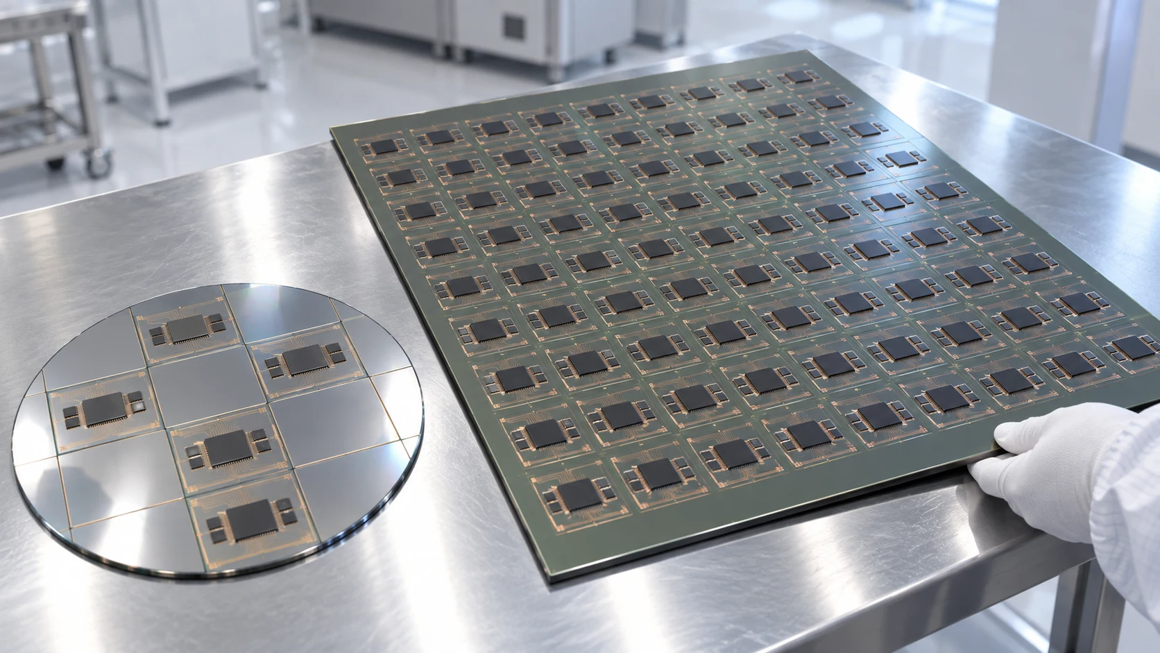
- What CoPoS is (the short version)
- How to read the name, and how it relates to CoWoS
- Why go from round to rectangular — our calculation
- What TSMC has said, and what it has not
- A materials engineer's view (1): what changes in the materials when the base becomes a panel
- What gets harder on a panel — exposure, planarisation, warpage
- A materials engineer's view (2): lowering warpage through the material
- Open issues — cautions when reading about CoPoS
- Glossary / References / Claim-to-source audit
Sourced = stated in published material from TSMC or another named source, or in a conference paper (link given)
Our calculation = a figure this article derived, with the assumptions spelled out
Not yet confirmed = a plan or a statement of intent, with no confirmed result behind it
Structural readings and materials-level interpretation are marked as our commentary. Where official material could not confirm a point, we write "could not be confirmed" rather than fill the gap with a guess.
1. What CoPoS is (the short version)
What the name tells you is the order of operations: handle the chips on a panel, then place the result on a substrate. It reads as CoWoS (Chip on Wafer on Substrate) with "wafer" replaced by "panel" (our commentary).
- What is confirmed officially: On 16 April 2026, TSMC Chairman and CEO C.C. Wei said on the earnings call that TSMC is working on CoPoS, is building a pilot line right now, expects production a couple of years later, and that the main supply today is still large-size CoWoSSourced
- How the timing is treated: Production was described only as "a couple of years later". No year was givenNot yet confirmed
- What could not be confirmed: the expanded name, the panel dimensions, the materials of the interposer layer and substrate core, the pilot line's location and start date, and customers. We found none of these in TSMC's official material
| Item | What we could confirm | Basis |
|---|---|---|
| TSMC is working on CoPoS | Confirmed | TSMC earnings call, 16 April 2026 [Reference 1] |
| Pilot line | Only a statement that it is being built. Location and start date could not be confirmed | Same [Reference 1] |
| Production timing | Only "a couple of years later". No year could be confirmed Not yet confirmed | Same [Reference 1] |
| Relationship to CoWoS | Discussed side by side; the main supply today is large-size CoWoS. Whether CoPoS replaces or supplements it could not be confirmed | Same [Reference 1] |
| Expanded name | Not found in TSMC's official material. This article uses Chip-on-Panel-on-Substrate only as a way of reading the name | Commentary |
| Panel dimensions | Could not be confirmed | — |
| Interposer-layer and substrate-core materials | Could not be confirmed (not even whether glass or organic) | — |
| Customers | Could not be confirmed. This article does not use customer names that appear only in press reports | — |
Many press reports give specific panel dimensions, sites, production years and customers for CoPoS. In the material we checked, though, none of those figures appear in TSMC's own public documents (earnings-call transcripts, website, press releases). This article does not use figures it cannot trace to official material. When you see a number, first check whether its source is an official document.
2. How to read the name, and how it relates to CoWoS
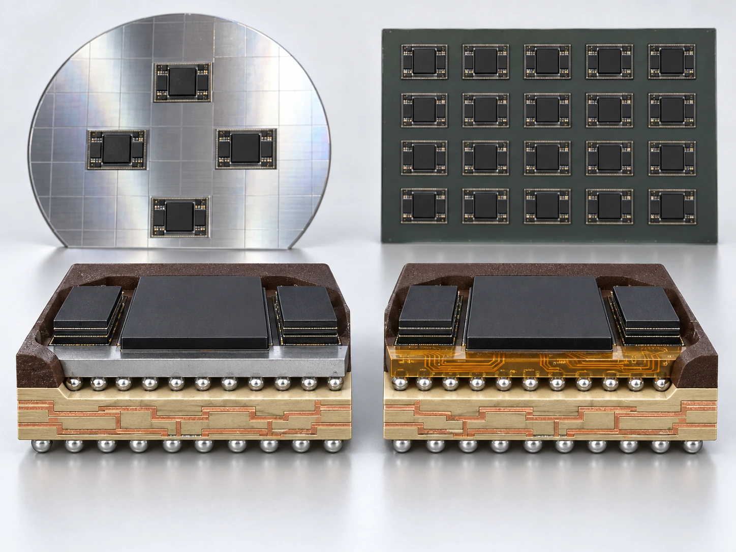
As our explainer on CoWoS showed, CoWoS spells out the assembly order: chips go onto a wafer (the interposer), the result is cut out, and it is placed on a substrate. CoPoS replaces the "wafer" with a "panel" (our commentary). We could not find the expanded form "Chip-on-Panel-on-Substrate" in the TSMC official material we checked. We use it here only as a widely used reading of the name.
What the three CoWoS variants suggest about fit with panels
TSMC's technology page describes the three CoWoS variants as followsSourced.
- CoWoS-S: a silicon interposer, up to 3.3 reticles (about 2,700 mm²)
- CoWoS-R: an RDL interposer made of polymer and copper traces and relatively flexible, which improves C4 joint integrity. Minimum 4 µm pitch (2 µm line width/spacing); in volume production since 2023
- CoWoS-L: an RDL-based interposer combined with local silicon interconnect (LSI) and other elements, described as a molding-based interposer. A 3.5-reticle version has been in volume production since 2024
Our commentary: a silicon plate can only be made in the shape of a round wafer, but polymer-and-copper wiring layers and molding resin are material systems that can also be handled on a rectangular surface. That organic, resin-based interposers are already in volume production in CoWoS-R and CoWoS-L could serve as a materials-side starting point for moving to panels. However, we could not confirm which variant CoPoS would build on.
Relationship to CoWoS: TSMC talks about them side by side
On the 16 April 2026 earnings call, an analyst asked whether, for larger sizes, TSMC meant CoPoS, CoWoS-L (2.5D), or 3D. The investor-relations officer relayed this as a question about larger reticle sizes, CoWoS-L or panel level, and Mr Wei answered along these linesSourced:
- TSMC supplies very large reticle-size CoWoS today
- It is also working on CoPoS. Taken together, the aim is to give customers enough capacity at a reasonable cost
- That is why a pilot line is being built now, with production a couple of years laterNot yet confirmed
- But the main supply today is still large-size CoWoS
The only link between CoPoS and "panel" in TSMC's own words is the investor-relations officer's rephrasing (panel level) on the call. We found no passage where TSMC itself describes CoPoS's structure or dimensions.
Whether CoPoS would replace or supplement CoWoS, TSMC has not said. In the same April 2026 symposium announcement, TSMC said CoWoS itself is already producing 5.5-reticle versions and plans a 14-reticle version for 2028Sourced (the plan is Not yet confirmed). At least for now, it reads as if the scaling of CoWoS and the preparation of CoPoS are going on in parallel (our commentary).
This article does not claim that wafer-based CoWoS or panel-based CoPoS is the better technology. We treat the differences as differences in structure, materials and process: the shape of the base (round or rectangular), the material and manufacture of the interposer layer, the exposure and planarisation methods, and how warpage appears. Because little about CoPoS can be confirmed officially, chapters 3 onward read "what is asked of a panel" from related research.
3. Why go from round to rectangular — our calculation
Cut square parts from a round wafer and the edge leaves scrap. In our explainer on PLP we calculated that for 50 mm square packages, a 510 × 515 mm panel yields about 4.8 times as many parts as a 300 mm wafer. Here we change the angle and redo the same calculation along the plan for ever-larger CoWoS interposers. TSMC has published plans to scale CoWoS to 5.5 reticles (in production), 9.5 reticles (volume production in 2027, per its April 2025 announcement) and 14 reticles (planned for 2028) [References 4, 11]Sourced (the plans are Not yet confirmed).
- Area: one reticle is about 830 mm², and 3.3 reticles about 2,700 mm² (TSMC)Sourced. Other sizes are 830 mm² times the reticle count
- Shape: each interposer is treated as a square of the same area (real ones are often rectangles)
- Wafer: 300 mm. Squares are laid on a grid, only cells whose four corners all lie inside the circle are counted, and the grid origin is searched in 1 mm steps for the maximum count
- Panels: parts packed edge to edge with no gaps. Edge exclusion, kerf and spacing between parts are ignored
- Panel dimensions: 320 × 320 mm and 510 × 515 mm. Both are sizes used in research on organic interposers on panels at ECTC 2026Sourced. They are not CoPoS panel dimensions
| CoWoS generation (including plans) | Area | Side of an equal-area square | 300 mm wafer | 320 × 320 mm | 510 × 515 mm |
|---|---|---|---|---|---|
| 3.3 reticles | about 2,700 mm² | about 52 mm | 17 parts (65%) | 36 parts (95%) | 81 parts (83%) |
| 5.5 reticles | about 4,565 mm² | about 68 mm | 9 parts (58%) | 16 parts (71%) | 49 parts (85%) |
| 9.5 reticles | about 7,885 mm² | about 89 mm | 5 parts (56%) | 9 parts (69%) | 25 parts (75%) |
| 14 reticles | about 11,620 mm² | about 108 mm | 2 parts (33%) | 4 parts (45%) | 16 parts (71%) |
All figures are Our calculation. Percentages in brackets are the share of the base's area covered by the parts that fit. The 3.3-reticle area is TSMC's published value [Reference 3]; the 14-reticle plan is from [Reference 4].
The table shows that a wafer becomes disadvantageous very quickly as the part grows. Area use falls from 65% at 3.3 reticles to 33% at 14 reticles (our calculation). The count falls from 17 to 2, and at 14 reticles only two parts fit inside the circle. That is why the scale-up of AI packages strengthens the case for panels (our commentary).
Yet a panel is not automatically better. A 320 × 320 mm panel holds a 3.3-reticle part (about 52 mm square) as a neat 6 × 6, 36 parts, reaching 95%. But it holds a 14-reticle part (about 108 mm square) as only 2 × 2, 4 parts, leaving a strip about 104 mm wide unused (45%). How well the base size divides into the part size changes the use of area a great deal.
This also matters to those who supply materials and equipment. If the panel size is not settled, neither the equipment nor the supply form of materials can be narrowed to one. At ECTC 2026, Resonac wrote of its research on organic interposers on panels in terms of "320 × 320 mm and 510 × 515 mm panels", naming two sizes [Reference 5]Sourced. The SEMI 3D20 standard covered in our PLP explainer aims at specifying panel dimensions, thickness, warpage and mass for just this reason [Reference 8]. Since the panel size CoPoS adopts could not be confirmed, the fact that surrounding industries keep more than one size in view reads as a direct sign of that uncertainty (our commentary).
More parts per panel also means more parts lost when one panel fails. With sixteen 14-reticle parts on a 510 × 515 mm panel, one bad panel costs sixteen parts (our calculation). As our PLP explainer discussed, the weight of yield is a challenge common to panel formats.
4. What TSMC has said, and what it has not
On CoPoS, the only TSMC primary source we could confirm is part of the earnings-call transcripts. We did not find the term CoPoS on the CoWoS technology page, in the symposium-related press releases of April 2025 and April 2026 [References 4, 11], or in the earnings-call transcripts of July and October 2025 and January and July 2026.
| Date | Venue | Content (in substance) | Label |
|---|---|---|---|
| 16 April 2026 | Earnings call, Q1 [Reference 1] | Asked how TSMC will handle larger sizes, Mr Wei said TSMC supplies very large reticle-size CoWoS, is also working on CoPoS, is building a pilot line now and expects production a couple of years later. Today's main supply is large-size CoWoS | Sourced (statement) Not yet confirmed (production timing) |
| 16 April 2026 | Same [Reference 1] | Asked whether SoIC or panel-level packaging can solve issues such as warpage, Mr Wei said the challenges of advanced packaging are mechanical stress (warpage) and thermal limits, and that TSMC has experience of tackling them as die size grows. Panels were not singled out | Sourced (statement) |
| April 2026 | Symposium-related press release [Reference 4] | 5.5-reticle CoWoS in production; 14-reticle CoWoS planned for 2028. No mention of panels or CoPoS | Sourced Not yet confirmed (2028) |
| 16 July 2026 | Earnings call, Q2 [Reference 2] | Asked about progress on glass substrates, glass cores and the like, Mr Wei said most volume is still CoWoS, that TSMC is developing an alternative to lower cost and working with substrate makers, and that the line announced earlier needs about another year to mature (the transcript's word is "pipeline"). The term CoPoS was not used | Sourced (statement) Not yet confirmed (about one year) |
The transcripts are edited by LSEG and published by TSMC. The content above is a summary in substance, not a verbatim quotation.
How to read the July 2026 remark
The Q2 question was about glass substrates, glass cores and glass carriers. The term CoPoS appears in neither the question nor the answer. The "alternative" and the "line announced earlier" in the reply may point to the pilot line mentioned in April, but the transcript alone does not settle it. The transcript's word is "pipeline", and we could not confirm whether that is a transcription variant of "pilot line". This article uses the remark only to the extent that TSMC said it is developing an alternative around substrates and that it needs about a year to mature, and it does not tie that to CoPoS's timing.
What could not be confirmed (summary)
- The expanded name (whether Chip-on-Panel-on-Substrate is the official spelling)
- Panel dimensions, panel material (glass or organic), the structure of the interposer layer and its wiring method
- The pilot line's location and start date, the production year, and the production site
- Customers
- TSMC's policy on replacing or coexisting with CoWoS (beyond "the main supply is large-size CoWoS for now")
- Any TSMC conference paper on CoPoS (in the ECTC 2026 programme highlights we checked, we found no TSMC paper on CoPoS; TSMC's papers there concerned CoWoS reliability)
Trade press has also reported remarks said to have been made by TSMC executives in Q&A after the symposium. Because we could not confirm them in official slides or transcripts, we do not use them.
5. A materials engineer's view (1): what changes in the materials when the base becomes a panel
CoPoS's material composition has not been published. So we take a generic stack of chips + an interposer layer made on a panel + a package substrate, and sort out where materials and process issues would appear, using only what primary sources support.
| Location | What TSMC describes for wafer-based CoWoS | What a panel puts in question (commentary) | What primary sources confirm |
|---|---|---|---|
| ① Molding compound | L: a molding-based interposer [Reference 3]. A TSMC paper slated for ECTC 2026 names interface delamination between molding compound and silicon (at die corners) as a concern in CoWoS [Reference 5] | With more resin area, cure shrinkage, CTE and modulus bear directly on warpage and shifting of parts | A paper on low-warpage molding compound for FOPLP [Reference 7]. Use in CoPoS could not be confirmed |
| ② ③ Interposer layer (wiring) | S: silicon. R: polymer-and-copper wiring, minimum 4 µm pitch. L: RDL-based plus LSI [Reference 3] | Exposure, plating and planarisation of the wiring layers have to be uniform over a large rectangular area, keeping the surface flat without the stiffness of silicon | Several ECTC 2026 papers on organic interposers on panels [Reference 5]. The approach used in CoPoS could not be confirmed |
| Carrier and the panel itself | — | The stiffness, flatness and weight of the plate that holds the panel during manufacture. The larger it is, the more self-weight matters | Warpage and die-shift analysis on a glass carrier (550 × 650 mm) [Reference 6]. Not confirmed for CoPoS |
| ④ C4 bumps and reflow | The compliance of the RDL improves C4 joint integrity. The RDL layers and the C4/underfill buffer the CTE mismatch between SoC and substrate [Reference 3] | With a larger interposer layer, the absolute size of the in-plane expansion mismatch during reflow grows (see the calculation in chapter 6) | Only the wafer-based description. Panel-based could not be confirmed |
| ⑤ Package substrate (core + build-up) | — (TSMC says it works with substrate makers [Reference 2]) | On large packages the substrate's own warpage also dominates. Whether the core is organic or glass changes the stiffness and CTE design (see our explainers on package substrates and glass substrates) | The material of CoPoS's substrate core could not be confirmed |
The "wafer-based" and "primary sources" columns are Sourced (as stated in each document). The "what a panel puts in question" column is our commentary.
In wafer-based CoWoS-S, the silicon interposer itself is stiff and flat, and it is the base for the wiring. For larger interposers, TSMC points to the softer RDL interposer (CoWoS-R) and says that its compliance improves C4 joint integritySourced. In other words, during scale-up TSMC has already been moving its design from "take the load with a stiff base" to "let a compliant layer absorb the stress" (our commentary).
On a panel, what carries flatness and stiffness is no longer silicon but the panel itself (carrier or core) and the resin layers on it. Because the resin area grows, the design variables that matter shift toward shrinkage, CTE, glass transition temperature and modulus, all of which act directly on warpage. The glass cores and ceramic-dispersed cores in our explainer on glass substrates come up in exactly this context. Yet whether CoPoS uses glass or organic material could not be confirmed officially.
One more point. A TSMC reliability study on CoWoS slated for ECTC 2026 identifies interface delamination between molding compound and silicon at die corners, and says that interposer stiffness helps mitigate it [Reference 5]Sourced. Making the interposer softer and relying on stiffness to mitigate stress could be a design trade-off. That is a point we read by turning the paper's statement around; it is not the paper's own claim (our commentary).
6. What gets harder on a panel — exposure, planarisation, warpage
From here we turn to conference papers on interposer layers on panels. None of them is about CoPoS; they are studies of organic interposers on panels and of FOPLP (fan-out panel-level packaging). They are not material that shows CoPoS's challenges directly. Read them as references for what kinds of difficulty appear when work moves to a panel. The ECTC 2026 items below rest on the programme highlights published before the conference (dated 20 May 2026); we did not consult the full papers.
(1) Exposure: stitch fields together, or expose one large field
In wafer-based CoWoS, TSMC built interposers larger than a reticle with its own mask stitching, joining exposure fields (see our CoWoS explainer). Panels face the same problem. USHIO is scheduled to present at ECTC 2026 a method that exposes an area equivalent to 18 reticles in one go, with no stitching, on a 510 × 515 mm glass substrate, forming 1.5 µm line/space (L/S) patternsSourced. The programme highlights say this area is more than four times that of conventional substrate steppers, and that the process margin (22 µm) tolerates the usual thickness variation of organic and glass substrates [Reference 5].
From a materials standpoint, what matters here is thickness variation of the substrate. Since the range over which exposure stays in focus is limited, the flatness and thickness uniformity of the panel become, in effect, the quality of the panels and films that materials makers supply (see our PLP explainer; our commentary).
(2) Planarisation: flattening copper, barrier metal and polymer together
Resonac is scheduled to present at ECTC 2026 results in which organic-polymer damascene wiring at L/S 2/2 µm on 320 × 320 mm glass panels was planarised with panel-level CMP (chemical mechanical polishing)Sourced. The stated background is that as interposers grow to the 9.5-reticle class, the effective area of a round 300 mm wafer becomes the limit, and that the damascene process is expected to deliver the finer copper wiring HBM4 requires. A two-step CMP (bulk copper removal, then barrier metal) is reported to have brought the co-planarity at the Cu/Ti/polymer interfaces below 100 nm, with a post-CMP step height below 100 nm at L/S 2/2 µm [Reference 5].
Copper, barrier metal and polymer are very different in hardness and in how they polish. When you flatten the same surface, the softer material can be over-polished ("dishing"), and dense wiring areas can be polished away too much ("erosion"). The paper says it secured in-plane wiring uniformity by optimising the groove design of the polishing pad and the flow distribution of the slurry [Reference 5]Sourced. On a panel this has to be matched across a surface hundreds of millimetres wide. It is an area where the consumables (pads and slurry) and the design of the resin and metals being polished are questioned together (our commentary).
For reference, TSMC gives the minimum pitch of CoWoS-R as 4 µm (L/S 2/2 µm) [Reference 3]Sourced. That equals Resonac's 2/2 µm numerically, but the two values differ in what was measured and why, and neither is a CoPoS specification. You cannot infer CoPoS's wiring density from the coincidence of the numbers.
(3) Warpage: CTE mismatch, resin shrinkage and self-weight
Panel warpage cannot be explained by a single cause. Drawing on FOPLP research and on this series, we list three.
- Expansion mismatch between materials: layers with different CTE bow with every temperature change (see our explainer on CTE)
- Cure shrinkage of resin: the molding compound that embeds the chips shrinks as it hardens, and the panel warps [Reference 7]
- Self-weight and how the panel is held: A*STAR's Institute of Microelectronics (IME) in Singapore studied the dominant factors of warpage at each process step with finite element analysis and the Taguchi method, for mold-first FOPLP on a 550 × 650 mm glass carrier. It reports that warpage falls markedly when the panel lies on a table under its own weight, but rises when it is supported only along its edges, which makes handling thin panels a problem [Reference 6]Sourced
The third point is important because it does not look like a "materials problem". The larger and thinner a panel gets, the more the way it is held and set down enters into warpage as a quality issue. For materials suppliers, that means the choice of core and carrier thickness and stiffness has to be made together with the equipment side's handling design (our commentary). A review of FOPLP (Lau, 2019) likewise lists warpage and the type of temporary carrier (wafer or panel) among its main topics [Reference 10].
The displacement from an expansion mismatch is proportional to distance. Here we calculate the free-expansion difference from the centre to the edge for a CTE difference of 1 ppm/K and a temperature change of 235 KOur calculation.
| Position measured from the centre | Distance | Displacement per 1 ppm/K of CTE difference |
|---|---|---|
| Edge of a 300 mm wafer | 150 mm | about 35 µm |
| Middle of an edge of a 320 × 320 mm panel | 160 mm | about 38 µm |
| Middle of an edge of a 510 × 515 mm panel | 255 mm | about 60 µm |
| Corner of a 510 × 515 mm panel | about 362 mm | about 85 µm |
Assumptions and limits: the 235 K change is cooling from a reflow peak of about 260 °C to 25 °C (the same assumption as in our CTE explainer). Displacement = distance × CTE difference × temperature change, which assumes the layers expand and contract completely freely and so is an upper-bound-style figure. In reality the layers constrain one another, so much of the mismatch becomes stress rather than displacement. Also, the temperatures at which wiring layers form and at which layers become fixed differ by process, so this temperature change does not apply as is. Even so, for the same CTE difference, the corner of the panel is pushed about 2.4 times as far as the edge of the wafer, and that proportionality stands (85 ÷ 35). With L/S of a few micrometres and bump pitches of a few tens of micrometres, a displacement of tens of micrometres is not negligible (our commentary).
7. A materials engineer's view (2): lowering warpage through the material
Warpage can be tackled through equipment and handling, or through the material. An example of the latter is the molding material for FOPLP that Lintec reported at ECTC 2018Sourced [Reference 7]. The paper also notes, as background, that FOPLP uses substrate panels of about the same size as printed circuit board (PCB) manufacturing, so PCB lines can be partly reused and the initial investment in package manufacturing may be lower.
| Item | What the paper states |
|---|---|
| Aim | Cut panel warpage sharply without filling the molding layer heavily with silica particles |
| Materials approach | Part of the rigid molecular structure of the epoxy resin, a main component, was replaced stepwise with a softer, more flexible molecular chain |
| Effect | Strong stress relaxation at the glass transition temperature; through the viscoelasticity shown in the master curve, panel warpage was reduced to one fifth |
| Checking the trade-off | All the materials have a low glass transition temperature, yet die shear strength on silicon exceeded 50 N at 250 °C (5 × 5 mm² chip) and weight loss at 390 °C was under 5% |
| Reliability tests | Reflow after JEDEC moisture sensitivity level 2 conditions (85 °C, 60% RH, 168 hours), temperature cycling under JEDEC condition B (−55/+125 °C, 2,000 cycles), and board-level tests |
All of the above is Sourced (Kikuchi, Nedzu and Sugino, ECTC 2018 [Reference 7]; researchers at Lintec Corporation). It is a material for FOPLP, not for CoPoS.
When people think of low-warpage molding compounds, loading the resin heavily with inorganic filler such as silica to lower CTE comes to mind. The paper's wording, "without highly filling silica particles", signals a different route: putting soft chains into the molecular structure of the resin itself so that stress relaxes near the glass transition temperature (our commentary).
That route has a cost. The paper states plainly that the materials have a low glass transition temperature, and then confirms that adhesion and heat resistance are retained. Lowering the glass transition temperature is therefore a design change that can affect stiffness and reliability at high temperature, and has to be checked through measurement (our commentary). Just as the imec results in our PLP explainer concerned a combination that reached as far as the transparency of the temporary adhesive and the supply form of the molding material, panel materials development turns on a balance of several properties, not a single one.
This is a 2018 result for FOPLP materials, and this paper cannot tell us whether it would meet the requirements of CoPoS or of today's large AI packages. We could not confirm any information on CoPoS's molding compound published by TSMC or by materials suppliers.
8. Open issues — cautions when reading about CoPoS
(1) Little is confirmed officially
As of this writing (October 2026), what TSMC has said publicly about CoPoS centres on short remarks on earnings calls. Dimensions, timing, customers and materials beyond that could not be confirmed in TSMC's public material. When an article or slide deck gives numbers for CoPoS, read it with an eye to whether the source is TSMC's own documents, or another company's announcement, or a press report.
(2) Size and fineness together
ASE uses its panel-level fan-out with 300 × 300 mm panels for high-density products (chip-last) and 600 × 600 mm panels for low-density products (chip-first) [Reference 9]Sourced. As our fan-out explainer showed, the larger the panel, the harder warpage and positional accuracy become, and the harder it is to keep wiring fine. Resonac's 2/2 µm (320 × 320 mm) and USHIO's 1.5 µm (510 × 515 mm) are research and demonstration values; they are neither figures achieved on production lines nor CoPoS figures.
(3) The weight of yield
The more parts a panel carries, the more a single bad panel costs. With sixteen 14-reticle parts on a 510 × 515 mm panel, one failure loses sixteen (our calculation). What sits on it are chips already confirmed good. Yield over a large area probably remains a challenge for CoPoS to the end (our commentary).
(4) Equipment and standards
Equipment built for round wafers cannot be used on rectangular panels as it is. SEMI 3D20 specifies panel dimensions, thickness, warpage and mass, on the premise that numerous panel sizes are under investigation [Reference 8]Sourced. While CoPoS's dimensions are unpublished, equipment and materials suppliers around it have to keep more than one size in view (our commentary).
(5) Heat
Mr Wei cited thermal limits, alongside mechanical stress (warpage), as a challenge of advanced packaging [Reference 1]Sourced. The larger the package, the more it matters how the heat is removed. Heat is not specific to panels, but the balance of thermal conductivity and CTE stays at the centre of design on any base.
- Confirmed: TSMC is working on CoPoS, is building a pilot line and expects production a couple of years later. The main supply today is large-size CoWoSSourced. The production timing is Not yet confirmed
- Not confirmed: the expanded name, panel dimensions, materials (glass or organic), site, production year, customers
- From round to rectangular: for a 14-reticle part (about 108 mm square), a 300 mm wafer holds 2 parts with 33% area use, and a 510 × 515 mm panel holds 16 with 71%Our calculation. A 320 × 320 mm panel holds only 4 at 45%, so how the sizes match matters
- Materials issues: exposure and planarisation of the interposer layer, cure shrinkage and warpage of the molding compound, the substrate core, and C4 and reflow. There is related research on each, but use in CoPoS could not be confirmed
- Warpage can be lowered through the material too: one route is to put soft chains into the molecular structure of the molding compound (for FOPLP, 2018)
- Check the source of every number: do not use dimensions, dates or customers that cannot be traced to official material
9. Glossary
- CoPoS
- A panel-based advanced packaging effort TSMC has said it is working on. The expanded name is not confirmed in official material (read as Chip-on-Panel-on-Substrate).
- CoWoS
- Chip on Wafer on Substrate. TSMC's 2.5D advanced packaging technology, in S, R and L variants.
- Panel
- A large rectangular base used in place of a round wafer. Made of glass, organic materials or others.
- FOPLP
- Fan-Out Panel Level Packaging. Making fan-out packages on a panel.
- Pilot line
- A small-scale trial line used to verify processes and equipment before volume production.
- Interposer
- The intermediate layer that carries chips and interconnects them. Made either of silicon or of RDL.
- RDL
- Redistribution layer. A thin wiring layer made of polymer and copper.
- LSI (local silicon interconnect)
- A piece of silicon interconnect embedded only where needed in CoWoS-L.
- Reticle
- The area a scanner can print in one exposure. TSMC puts one reticle at about 830 mm².
- EMC
- Epoxy molding compound. Embeds and protects the chips, and also acts as a structural material.
- CMP
- Chemical mechanical polishing. Flattening a surface with chemicals and a polishing pad.
- Damascene wiring
- Wiring made by etching trenches into an insulating layer, filling them with copper and polishing away the excess.
- Dishing and erosion
- In CMP, the softer wiring areas dipping below the surface (dishing), and dense wiring areas being polished away too far (erosion).
- Die shift
- The displacement of placed chips caused by the flow and shrinkage of resin.
- CTE
- Coefficient of thermal expansion. The mismatch between materials produces warpage and stress.
- Glass transition temperature (Tg)
- The temperature at which a resin changes from a hard state to a soft one.
- C4 bump
- The solder bump connecting the interposer to the package substrate.
- SEMI 3D20
- The SEMI standard specifying panel outline dimensions, thickness, warpage and mass for PLP applications.
10. References
- TSMC "Q1 2026 Earnings Conference Transcript", 16 April 2026 (PDF) — investor.tsmc.com
- TSMC "Q2 2026 Earnings Conference Transcript", 16 July 2026 (PDF) — investor.tsmc.com
- TSMC "CoWoS®" technology page — 3dfabric.tsmc.com
- TSMC "TSMC Debuts A13 Technology at 2026 North America Technology Symposium", April 2026 — pr.tsmc.com
- IEEE ECTC "2026 ECTC Technical Tipsheet", dated 20 May 2026 (PDF; includes Resonac Paper 14.2, USHIO Paper 28.2, TSMC Paper 6.3 and others) — ectc.net
- Che, Yamamoto and Rao (A*STAR IME) "Panel Warpage and Die Shift Simulation and Characterization of Fan-Out Panel-Level Packaging", 2020 IEEE 70th ECTC (DOI 10.1109/ECTC32862.2020.00325) — ieeexplore.ieee.org
- Kikuchi, Nedzu and Sugino (Lintec) "Warpage Analysis with Newly Molding Material of Fan-Out Panel Level Packaging and the Board Level Reliability Test Results", 2018 IEEE 68th ECTC (DOI 10.1109/ECTC.2018.00149) — ieeexplore.ieee.org
- SEMI "SEMI 3D20 — Specification for Panel Characteristics for Panel Level Packaging (PLP) Applications" — store-us.semi.org
- ASE "Fan-Out Packaging" — ase.aseglobal.com
- John H. Lau "Recent Advances and Trends in Fan-Out Wafer/Panel-Level Packaging", Journal of Electronic Packaging 141(4), 2019 (DOI 10.1115/1.4043341) — doi.org
- TSMC "TSMC Unveils Next-Generation A14 Process at North America Technology Symposium", 23 April 2025 — pr.tsmc.com
11. Claim-to-source audit
| Claim in the text | Basis | Label |
|---|---|---|
| On the 16 April 2026 earnings call, an analyst asked whether larger sizes meant CoPoS, CoWoS-L or 3D; the investor-relations officer rephrased it as "CoWoS-L or panel level"; and Mr Wei replied that TSMC supplies very large reticle-size CoWoS, is also working on CoPoS, is building a pilot line now to give customers enough capacity at a reasonable cost, and expects production a couple of years later. The main supply today is large-size CoWoS | TSMC Q1 2026 earnings-call transcript (16 April 2026)[Reference 1] https://investor.tsmc.com/english/encrypt/files/encrypt_file/reports/2026-04/3cef85204275f94fd111485cfdf4adb3c0263c45/TSMC%201Q26%20Transcript.pdf | Sourced |
| Production timing was given only as "a couple of years later", with no year | TSMC Q1 2026 earnings-call transcript. A statement of intent, not a result[Reference 1] https://investor.tsmc.com/english/encrypt/files/encrypt_file/reports/2026-04/3cef85204275f94fd111485cfdf4adb3c0263c45/TSMC%201Q26%20Transcript.pdf | Not yet confirmed |
| Asked whether SoIC or panel-level packaging could solve issues such as warpage, Mr Wei said mechanical stress (warpage) and thermal limits are the challenges of advanced packaging and that TSMC has experience tackling them while increasing die size. Panels were not singled out | TSMC Q1 2026 earnings-call transcript[Reference 1] https://investor.tsmc.com/english/encrypt/files/encrypt_file/reports/2026-04/3cef85204275f94fd111485cfdf4adb3c0263c45/TSMC%201Q26%20Transcript.pdf | Sourced |
| On the 16 July 2026 earnings call, asked about progress on glass substrates and glass cores, Mr Wei said most volume is still CoWoS, an alternative to lower cost is being developed with substrate makers involved, and the line announced earlier (the transcript says "pipeline") needs about another year to mature. The term CoPoS was not used | TSMC Q2 2026 earnings-call transcript (16 July 2026)[Reference 2] https://investor.tsmc.com/english/encrypt/files/encrypt_file/reports/2026-08/3e494f0c14dd0890f897aa044415e21d93486cc4/TSMC%202Q26%20Transcript.pdf | Sourced |
| The outlook of "about one year" to maturity | TSMC Q2 2026 earnings-call transcript. A plan, not a result[Reference 2] https://investor.tsmc.com/english/encrypt/files/encrypt_file/reports/2026-08/3e494f0c14dd0890f897aa044415e21d93486cc4/TSMC%202Q26%20Transcript.pdf | Not yet confirmed |
| CoWoS-S goes up to 3.3 reticles (about 2,700 mm²). CoWoS-R is a polymer-and-copper RDL interposer, relatively flexible, improving C4 joint integrity; minimum 4 µm pitch (L/S 2/2 µm); in volume production since 2023; the RDL layer and C4/underfill buffer the CTE mismatch between SoC and substrate. CoWoS-L combines an RDL-based interposer with LSI and other elements, has a molding-based interposer, and a 3.5-reticle version has been in volume production since 2024. CoWoS has been in production since 2012 | TSMC CoWoS technology page[Reference 3] https://3dfabric.tsmc.com/english/dedicatedFoundry/technology/cowos.htm | Sourced |
| One reticle is about 830 mm² | TSMC CoWoS technology page (this article computes other generations as 830 mm² times the reticle count)[Reference 3] https://3dfabric.tsmc.com/english/dedicatedFoundry/technology/cowos.htm | Sourced |
| The April 2026 symposium-related announcement: 5.5-reticle CoWoS in production; 14-reticle CoWoS (about 10 compute dies and 20 HBM) planned for 2028. No mention of panels or CoPoS | TSMC press release, April 2026[Reference 4] https://pr.tsmc.com/english/news/3302 | Sourced |
| The 14-reticle version is planned for 2028 | TSMC press release. A plan, not a result[Reference 4] https://pr.tsmc.com/english/news/3302 | Not yet confirmed |
| The April 2025 announcement planned volume production of 9.5-reticle CoWoS in 2027 and made no mention of panels or CoPoS | TSMC press release, 23 April 2025[Reference 11] https://pr.tsmc.com/english/news/3228 | Sourced |
| The term CoPoS does not appear in the July and October 2025 or January and July 2026 earnings-call transcripts (the January 2026 transcript contains an analyst's mention of "panel") | TSMC earnings-call transcripts (our full-text search of each)[Reference 1] https://investor.tsmc.com/english/encrypt/files/encrypt_file/reports/2026-04/3cef85204275f94fd111485cfdf4adb3c0263c45/TSMC%201Q26%20Transcript.pdf[Reference 2] https://investor.tsmc.com/english/encrypt/files/encrypt_file/reports/2026-08/3e494f0c14dd0890f897aa044415e21d93486cc4/TSMC%202Q26%20Transcript.pdf | Sourced |
| That the organic, resin-based materials of CoWoS-R and CoWoS-L (polymer-and-copper wiring, molding resin) can also be handled on a rectangular surface. Which variant CoPoS builds on could not be confirmed | Our reading of the published material. Not a view stated by TSMC or anyone else | Commentary |
| At ECTC 2026 Resonac names two sizes for panel research on organic interposers, "320 × 320 mm and 510 × 515 mm". When interposers reach 9.5 reticles the effective area of a round 300 mm wafer becomes the limit. On 320 × 320 mm glass panels it planarised L/S 2/2 µm organic-polymer damascene wiring with two-step CMP, with Cu/Ti/polymer co-planarity and post-CMP step height under 100 nm, optimising pad groove design and slurry flow (Paper 14.2) | ECTC 2026 Technical Tipsheet (dated 20 May 2026)[Reference 5] https://ectc.net/wp-content/uploads/2023/03/2026-ECTC-REVISED-Technical-Tipsheet-with-images.pdf | Sourced |
| At ECTC 2026 USHIO exposes an area of 18 reticles in one shot, without stitching, on 510 × 515 mm glass, forming 1.5 µm L/S. The area is more than four times that of conventional substrate steppers; the process margin of 22 µm tolerates the usual thickness variation of organic and glass substrates (Paper 28.2) | ECTC 2026 Technical Tipsheet[Reference 5] https://ectc.net/wp-content/uploads/2023/03/2026-ECTC-REVISED-Technical-Tipsheet-with-images.pdf | Sourced |
| At ECTC 2026 TSMC reports that interface delamination between the molding compound (EMC) and silicon at die corners is a dominant concern in CoWoS and that interposer stiffness helps mitigate CTE mismatch (Paper 6.3). No TSMC paper on CoPoS appears in the tipsheet | ECTC 2026 Technical Tipsheet. We consulted the descriptions of the papers, not the full papers[Reference 5] https://ectc.net/wp-content/uploads/2023/03/2026-ECTC-REVISED-Technical-Tipsheet-with-images.pdf | Sourced |
| Study by A*STAR IME: for mold-first FOPLP on a 550 × 650 mm glass carrier, finite element analysis and the Taguchi method were used to identify the dominant factors of warpage and die shift at each process step, with reductions through structure design, process optimisation and material selection. Modelling self-weight, warpage falls markedly when the panel lies on a table and rises when supported along its edges, making thin-panel handling a problem | Che, Yamamoto and Rao, ECTC 2020 (IEEE Xplore)[Reference 6] https://ieeexplore.ieee.org/document/9159466 | Sourced |
| Study by Lintec: a molding material that sharply lowers panel warpage without heavy silica filling. Part of the epoxy resin's rigid structure was replaced with flexible chains, giving strong stress relaxation at the glass transition temperature and one-fifth the warpage. Low glass transition temperature, but die shear strength above 50 N at 250 °C (5 × 5 mm²) and weight loss under 5% at 390 °C. Reflow after MSL 2, JEDEC condition B temperature cycling (−55/+125 °C, 2,000 cycles) and board-level tests were carried out. The paper also says FOPLP and PCB manufacturing use similar panel sizes, so PCB lines may be partly reused | Kikuchi, Nedzu and Sugino, ECTC 2018 (IEEE Xplore)[Reference 7] https://ieeexplore.ieee.org/document/8429662 | Sourced |
| SEMI 3D20 specifies panel outline dimensions, thickness, warpage and mass for PLP applications; the current revision is 3D20-0921; numerous panel sizes are under investigation | SEMI 3D20 standard information page[Reference 8] https://store-us.semi.org/products/3d02000-semi-3d20-en-specification-for-panel-characteristics-for-panel-level-packaging-plp-applications | Sourced |
| ASE uses 300 × 300 mm panels for high-density (chip-last) and 600 × 600 mm panels for low-density (chip-first) panel-level fan-out | ASE Fan-Out Packaging[Reference 9] https://ase.aseglobal.com/fan-out-packaging/ | Sourced |
| A review of FOPLP lists warpage and the type of temporary carrier (wafer or panel) among its main topics | Lau, J. Electron. Packag. 141(4), 2019[Reference 10] https://doi.org/10.1115/1.4043341 | Sourced |
| Part counts and area use (17 / 36 / 81, 9 / 16 / 49, 5 / 9 / 25 and 2 / 4 / 16 parts, and so on). Area = 830 mm² times the reticle count (3.3 reticles = 2,700 mm²), equal-area squares, grid layout on a 300 mm wafer with all four corners inside the circle and the origin searched in 1 mm steps, parts packed from one edge on panels, with edge exclusion, kerf and gaps ignored. The panel sizes 320 × 320 mm and 510 × 515 mm are sizes from research and are not CoPoS dimensions | Our calculation from one reticle = 830 mm², 3.3 reticles = 2,700 mm² (TSMC published values) and the 150 mm radius of a 300 mm wafer | Our calculation |
| With sixteen 14-reticle parts on a 510 × 515 mm panel, one bad panel costs sixteen parts | Our calculation from the count of 16 parts above | Our calculation |
| Free-expansion difference per 1 ppm/K of CTE mismatch and a 235 K change: about 35 µm at 150 mm, 38 µm at 160 mm, 60 µm at 255 mm and 85 µm at the corner, about 362 mm away (√(255² + 257.5²)). The corner is about 2.4 times the wafer edge | Our calculation: displacement = distance × CTE difference × temperature change. The 235 K is cooling from a reflow peak of about 260 °C to 25 °C (same assumption as our CTE explainer), assuming completely free expansion. In reality the layers constrain one another and the mismatch becomes stress | Our calculation |
| That the count of parts is set by how the panel and part sizes divide, so a panel is not always advantageous; and that an undecided panel size prevents equipment and material supply forms from being narrowed | Our reading of the calculation above and of the published material | Commentary |
| The shift in design from a stiff base to a compliant layer; the reading that on a panel the panel itself and the resin layers on it carry flatness and stiffness; and the reading that making the interposer softer and relying on stiffness for mitigation could be a trade-off | Our interpretation of the published material. Not claims made by the papers or the companies | Commentary |
| Exposure fields, the relationship between substrate thickness variation and focus, how copper, barrier metal and polymer polish differently, the two routes to a low-warpage molding compound (lower the CTE, or relax stress), and the way handling conditions enter into warpage | Commentary based on general relationships in materials engineering and process technology. No numerical claim is made about any specific product | Commentary |
| The expanded name (Chip-on-Panel-on-Substrate) | Not confirmed in TSMC's official material (transcripts, technology page, press releases), so we do not assert it as the official spelling. We use it only to explain how the name reads | Commentary |
| CoPoS panel dimensions; the materials of the panel, interposer layer and substrate core (glass or organic); the pilot line's location and start date; the production year and site; customers; the policy on replacing or coexisting with CoWoS; any TSMC conference paper on CoPoS | Could not be confirmed in TSMC's public material, so not stated. Figures and customer names reported in the press are not used because they cannot be traced to official material | Commentary |
| That the CoPoS pilot line has started operating, or that volume production has begun | Our note: as of this writing (October 2026), we found no TSMC primary source showing a result | Not yet confirmed |
| That Figs. 1, 3, 4, 5 and 6 are explanatory drawings, not real structure diagrams or design drawings, and that the hero image and Fig. 2 are AI-generated | Note by this article | Commentary |
Last updated 3 October 2026. Sources are limited to TSMC's earnings-call transcripts, website and press releases, papers presented at IEEE ECTC, and published material from standards bodies and companies. Because the article includes structural readings and materials-level interpretation, those are labelled "commentary" and kept separate from sourced facts. The expanded name of CoPoS, panel dimensions, materials, the pilot line's location and start date, the production year, customers and any replacement relationship with CoWoS are not stated because they could not be confirmed in TSMC's public material. Conference papers are described only as far as their programme highlights or abstracts allow; we did not consult the full papers. The research discussed in chapters 6 and 7 concerns organic interposers on panels and FOPLP, not CoPoS. All figures are explanatory concept graphics. Figs. 1, 3, 4, 5 and 6 are vector drawings; the hero image and Fig. 2 are AI-generated images. None of them accurately represents real structures or dimensional ratios.