

Key Findings
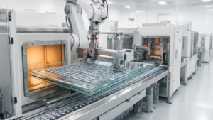
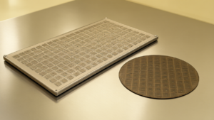
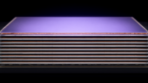
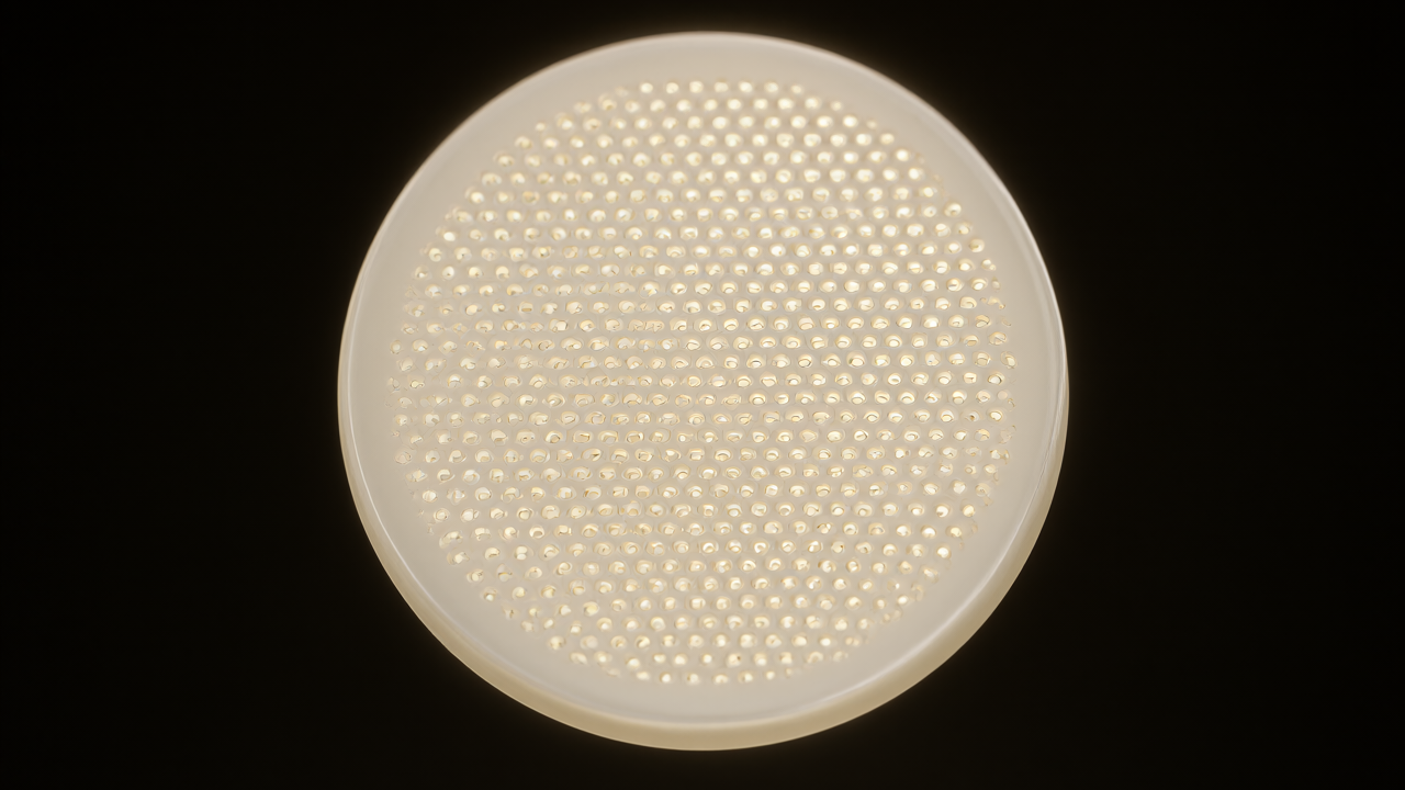
The Korea Institute of Ceramic Technology (KICET), in collaboration with HAS, Korea Aerospace University, and LX Glass, has developed a photosensitive crystallizable glass material and the associated processing technology required for next-generation semiconductor packaging. The team successfully fabricated large-area glass substrate specimens with a diameter of 200mm and verified the ability to form precise micro-holes (Through Glass Vias, or TGV) on 100mm-class substrates of the same material.
Technical Details
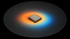
The developed photosensitive crystallizable glass is a specialized material that selectively forms crystals in areas exposed to ultraviolet (UV) light and subsequent heat treatment. The technical process encompasses the entire production chain, including:
- Raw material blending and glass substrate fabrication.
- UV irradiation and thermal treatment to induce selective crystallization.
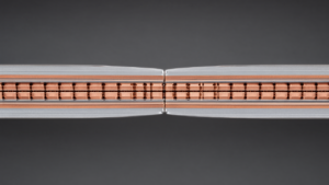
- Chemical etching to remove the crystallized portions, allowing for the precise creation of multiple micro-holes (TGV).
This method addresses the critical challenge of creating uniform, precise micro-holes in glass, which is traditionally difficult due to the material’s fragility and the precision required for vertical interconnects.
Background and Context
Glass substrates serve as the base for mounting and connecting semiconductor chips. Compared to conventional plastic-based substrates, glass offers a smoother surface and lower thermal deformation. These properties are advantageous for creating denser, smaller circuits and reducing electrical signal loss. However, the commercialization of glass substrates has been hindered by the material’s susceptibility to impact and the difficulty of achieving precise TGV processing.
Significance and Outlook
By securing the technology to design and manufacture photosensitive crystallizable glass, KICET has established a technical foundation for the localization of semiconductor packaging materials. Dr. Han Yun-su of KICET stated that the team intends to further refine large-area fabrication and micro-processing technologies to facilitate the industrial application and domestic production of next-generation semiconductor packaging materials.
Source: https://www.fnnews.com/news/202610291026456501
Get our weekly technology intelligence — free
Receive an infographic that lets you judge at a glance whether each field’s analysis report is worth reading.
Subscribe Free — Weekly Tech Intelligence
By subscribing, you’ll receive Troy-Technical’s weekly technology intelligence newsletter.
- Your email and selected fields are used only to deliver the newsletter.
- We never share your information with third parties.
- You can unsubscribe anytime via the link in each email.
See our Privacy Policy for details.
Takes about a minute · Unsubscribe anytime