TECHNOLOGY EXPLAINER
What a Via Is
— drill a hole, fill it with metal, and every difficulty that follows
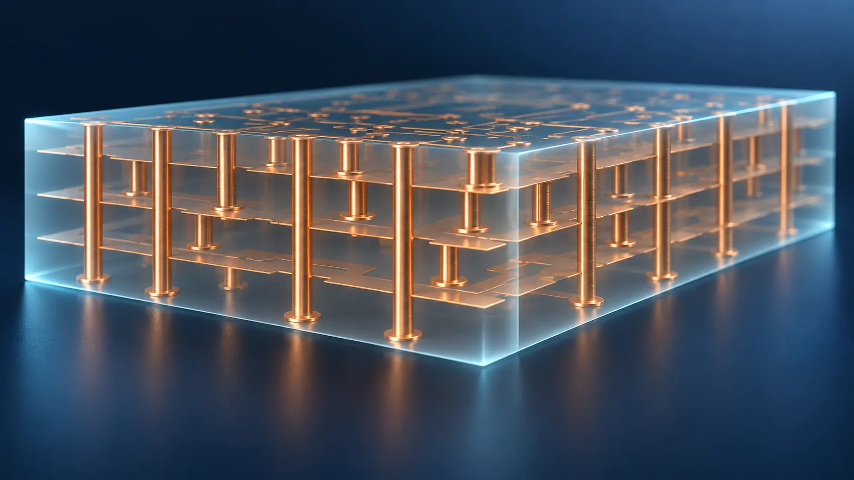
Wiring in one plane is not enough. A hole that connects layer to layer vertically is a via. What you do is simple: open a hole, clean it, fill it with metal. And yet those three steps rest on materials technologies from completely different fields — laser wavelength, resin surface roughness and plating-bath additives.
- What a via is (the short version)
- Kinds of via — all the way through, or stopping part way
- Opening the hole — what drills cover and what lasers cover
- A materials engineer's view 1: the wavelength chooses what gets removed
- What the hole leaves behind — desmear
- A materials engineer's view 2: the roughness versus adhesion trade-off
- Filling the hole — why it fills from the bottom
- What is still hard
- Glossary / Primary sources / Claim-to-source audit
Sourced = content stated in a company's published material or an academic paper (link given)
Our calculation = a figure this article derived, with the assumptions spelled out
Not yet confirmed = a plan with no confirmed track record
Beyond those, process framing and readings about materials design are marked Commentary.
1. What a via is (the short version)
A via is a hole that connects one layer of a board to another vertically, together with the conductor inside it. The word is Latin for "way": a route across layers.
- What it is for: one wiring layer is never enough, so stacked layers have to be joined up and down
- How it is made: three steps — open the hole, clean the inside, fill it with metal (usually copper)
- What is hard: the smaller and deeper the hole, the harder all three become
The word via gets a different name depending on the base material, and this series treats each separately.
- Through silicon = TSV, in the TSV article
- Through glass = TGV, in the Glass Substrate article
- Within a redistribution layer, formed in photosensitive resin, in the RDL article
This article deals with the ground common to all of them: the problem of opening a hole and filling it with metal. The examples are mostly organic (resin) substrates, but the thinking is the same whatever the base material.
2. Kinds of via — all the way through, or stopping part way
A via is named for what it connects to what. An article on Via Mechanics in the journal of the Japan Society of Mechanical Engineers distinguishes the machines as "drilling machines for through-holes, and laser machines for the non-penetrating blind holes in the inner layers of a board"Sourced. Whether it goes through or not changes even the equipment.
The point to hold on to is that a blind via has to stop part way. Drilling part way is hard to control in depth. Which is why lasers are used — but why can a laser stop at just the right place? That is the subject of Section 4.
3. Opening the hole — what drills cover and what lasers cover
There are broadly two ways to open a hole: a mechanical drill and a laser. And the two divide cleanly by the size of hole they can make.
Via Mechanics' drilling machines are stated to work from 0.1 to 6.35 mm on the standard machine and from 0.050 mm on the fine-diameter machine, with spindle speeds published as 160k and 200k rpm (standard) and 300k and 350k rpm (high speed)Sourced. The JSME journal article describes the company as having "achieved drilling of holes as small as 0.05 mm in diameter" with "positioning speeds of over 5000 Hz at maximum"Sourced.
4. A materials engineer's view 1: the wavelength chooses what gets removed
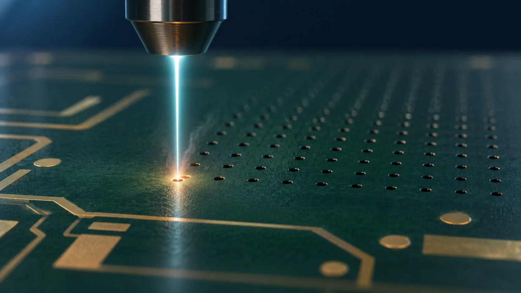
When you drill with a laser, which material is removed and which is not is decided by the wavelength. And a printed circuit board is made of three materials with different natures. The JSME journal article describes a board as having "three main constituents: copper, the epoxy resin dielectric layer, and glass"Sourced.
The same article says of the CO2 laser that "with a CO2 laser at around 9400 nm, the presence of copper makes that point a blind hole"Sourced.
Think about what is happening and it is inverted. "Copper does not absorb this wavelength" is, from a machining point of view, a defect. You cannot use the laser when you want to cut copper.
But when making a blind via, that defect becomes a stop, as a function. There is no need to measure depth and halt. The material halts it for you.
A UV laser, by contrast, is described in the same article: "ultraviolet light from a YAG laser at around 355 nm is strongly absorbed by epoxy resin and copper, while glass absorbs it weakly"Sourced. Because it cuts copper too, it can open smaller holes — the Fukuoka centre publishes 60 to 400 µm for CO2 against 8 to 68 µm for UVSourced.
"Strongly absorbed, therefore removable, therefore small" and "not absorbed, therefore a stop, therefore no depth control needed" are two sides of one coin. Which side you want depends on the via you are making (Commentary).
The same centre reports that adding an aperture to the UV laser to narrow the beam has pushed diameters down, with via top diameters of 8.3 to 22.5 µm and bottom diameters of 3.7 to 13.5 µm at aperture diameters of 49 to 59 µmSourced.
5. What the hole leaves behind — desmear
An open hole is not ready for metal. At the bottom sits a residue of melted resin, called smear.
Samco states that "organic residue (smear) at the bottom of the via hole after laser processing becomes a problem", and that it has conventionally been "cleaned with chemistries such as permanganate"Sourced.
That removal step is desmear. But desmear does not have only one job. Ushio describes it as "two processes: removing the smear from the blind via and forming roughness on the dielectric resin surface"Sourced.
6. A materials engineer's view 2: the roughness versus adhesion trade-off
Why go to the trouble of roughening the resin surface? Ushio's explanation is clear: "erosion of the surface by the desmear solution gives the electroless plating seed layer an anchor effect, raising the adhesion of the plated wiring"Sourced.
In other words, resin and copper do not bond chemically. You key the copper into the texture and hold it mechanically. That is the anchor effect.
Which creates a problem. The same company says "technology is needed that resolves the trade-off between surface roughness control and adhesion"Sourced.
Without roughness it will not stick; with roughness you cannot draw fine traces — the same shape recurs throughout this series.
- RDL: the finer the trace, the more the underlying roughness gets in the way
- Package Substrate: roughening the build-up material collides with finer line and space
- Build-up Film: changing the resin to lower Df costs you adhesion
At high frequency the skin effect keeps current near the conductor surface. The rougher that surface, the longer the path the current takes, and the higher the loss. So roughness not only obstructs fine wiring; it becomes loss in a fast signal in its own right (Commentary).
Ushio's photo-desmear uses 172 nm vacuum ultraviolet (VUV): "VUV light converts oxygen molecules to ozone, and the decomposition of that ozone generates reactive oxygen" which breaks down organic matter, after which "the inorganic residue is treated ultrasonically in pure water"Sourced. Not cutting away with chemistry, but decomposing with light and reactive oxygen. Changing the approach is an attempt at a different answer to the roughness-adhesion trade-off (Commentary).
The Fukuoka centre, reporting its results on small-diameter vias, notes that "for desmear, dry is preferable because a wet process widens the via diameter considerably"Sourced. Chemistry dissolves the hole wall too, so the small hole you worked to open grows back. Shrink the via and you are forced to revisit even the desmear method (Commentary).
7. Filling the hole — why it fills from the bottom
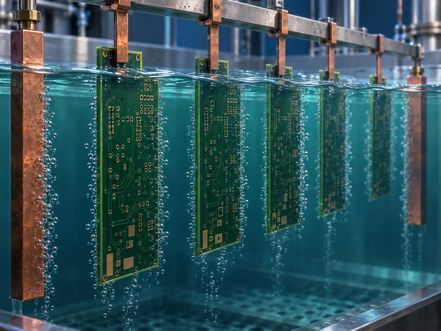
Into the clean hole goes the copper, by electrolytic plating. And here something counter-intuitive happens.
Plate normally and the hole closes from the top. Current gathers more readily at the mouth. Close the mouth first and a cavity is sealed inside.
A doctoral thesis submitted to Osaka Prefecture University (Taro Hayashi, February 2015) records the phenomenon: "In electrolytic copper plating of high-aspect-ratio vias, current concentration at the via opening readily accelerates deposition, so the via opening closes and defects called voids and seams occur inside the via"Sourced. And "the occurrence of voids and seams causes wiring failures in TSV interconnects"Sourced.
So you build in a mechanism that only speeds up the bottom
The same thesis states that "to achieve complete filling of the via, good via-filling behaviour known as bottom-up filling, in which the bottom of the via is plated preferentially, is required"Sourced.
What delivers it is the additives in the plating bath. Components with different jobs go in together.
On the accelerator mechanism, the thesis introduces the curvature-enhanced account of T. P. Moffat and colleagues: "as electrolytic copper plating proceeds, the electrode area at the bottom of the via or trench decreases. With that decrease in area, the accelerator concentration at the bottom of the via or trench increases"Sourced.
Which is neat. The more it fills, the faster it fills. Designing a chemical reaction, you normally dislike positive feedback because it runs away. In via filling, that runaway is exactly the function you want.
And the mechanism is geometric. The accelerator is not incorporated into the deposit but stays on the surface, so as the area shrinks, the same quantity of accelerator concentrates into a smaller space. Not molecular design of the additive, then: the shape of the hole itself is the accelerator (Commentary).
The leveller works the other way. According to the same thesis, diallylamine-type additives "adsorb mainly where the flow is fast, such as the upper part of the via and outside it"Sourced. They collect where the liquid moves fast and suppress it there. Where the accelerator takes its cue from area, the leveller takes its cue from flow velocity (Commentary).
What the dimensions actually are in practice
JCU, describing its via-filling copper sulphate plating "CU-BRITE VF7" for package substrates, shows an evaluation using microvias 60 µm and 50 µm in diameter and 30 µm deep, at 1.5 A/dm² and 15 µm of depositSourced. Of the filling principle it says "suppressing plating growth at the surface of the blind via hole and promoting growth inside fills the microvia with copper plating"Sourced. The company also states "three additive components are used; all components can be analysed by electrochemical measurement (CVS)", and that "wiring thickness uniformity is 40% better than the conventional process"Sourced.
Additives are consumed and degrade as plating proceeds. Let the concentrations drift and the hole stops filling from the bottom. So in volume production you have to measure the concentrations in the bath and keep topping them up.
JCU going out of its way to state "all components can be analysed by electrochemical measurement (CVS)" is because being controllable is itself the product's valueSourced. With an unmeasurable component in the bath, a problem cannot be traced to its cause (Commentary).
8. What is still hard
(1) The deeper and narrower the hole, the harder everything gets
The difficulty of a via is expressed by its aspect ratio, depth divided by diameter. A simple calculation shows what happens as it rises.
Take a cylindrical hole of diameter d and depth hOur calculation.
- Opening area = pi d² / 4
- Inner wall area = pi d h
- Their ratio = 4h/d = 4 × aspect ratio
So:
- Aspect ratio 0.5 (say 60 µm diameter, 30 µm deep): the wall is twice the opening
- Aspect ratio 2: eight times
- Aspect ratio 10: forty times
Assumptions: the hole is treated as a simple cylinder. Real laser vias are tapered, and TSVs are not perfect cylinders either.
What it shows is still plain. The opening that plating solution has to pass through stays small, while the wall that must be covered in copper keeps growing. Fresh solution does not reach the bottom, and reaction products do not get out. That imbalance between opening and interior is the essence of why high-aspect-ratio vias are hard to fill (Commentary).
For reference, JCU's evaluation conditions (50 to 60 µm diameter, 30 µm deep) correspond to an aspect ratio of 0.5 to 0.6Our calculation. The through-silicon vias in the TSV article, by contrast, aim at far higher aspect ratios.
(2) Make it smaller and the next step undoes it
Reporting vias in the 8 µm class made with a UV laser, the Fukuoka centre notes that "for desmear, dry is preferable because a wet process widens the via diameter considerably"Sourced. The effort of making the hole smaller is easily undone by the next step. As Samco points out, plasma treatment has the advantage that "no wet chemistry or expensive ancillary equipment is needed"Sourced.
(3) The leftover hole becomes an electrical nuisance
The last problem is neither mechanical nor chemical but electrical. Pass a signal into an intermediate layer through a plated through-hole and the rest of the barrel is left over. That is a stub.
RITA Electronics states that on a line with a stub "the impedance drops considerably", and that "at the frequency where that stub length corresponds to a quarter wavelength it acts as an antenna, resonance occurs, and transmission loss consequently deteriorates markedly"Sourced. The remedy, back-drilling, is "a method that controls the depth from the surface of the printed board to the signal wiring layer and cuts the stub away with a drill", and in the experimental example it "improved transmission characteristics by about 20 dB at frequencies above 15 GHz"Sourced.

A via looks like nothing more than opening a hole and filling it with metal. In fact three materials technologies from quite different fields are wired in series.
- Opening: laser wavelength against each material's absorption. Copper not absorbing is itself the stop
- Cleaning: resin surface roughness against plating adhesion. Too smooth and nothing sticks; too rough and no fine traces
- Filling: bath additives. An accelerator that concentrates as area shrinks, and a leveller that settles where flow is fast
And at every stage you hit the same wall: go smaller and it suddenly gets harder. A small hole is hard to open, hard to clean and hard to fill. That is why via scaling is talked about as the bottleneck in substrate technology: all three tighten at once (Commentary).
9. Glossary
- Via
- The hole connecting one layer of a board to another vertically, and the conductor inside it.
- Through-hole
- A via passing through every layer of the board, usually drilled mechanically.
- Blind via
- A non-penetrating via from the surface to an inner layer.
- Buried via
- A via joining inner layers, invisible from outside the board.
- Stacked via
- Blind vias stacked directly above one another to make a deeper connection.
- Aspect ratio
- Via depth divided by diameter. Higher makes drilling, cleaning and filling all harder.
- Smear
- Melted resin residue left at the bottom of a via by drilling.
- Desmear
- The step that removes smear and roughens the resin surface at the same time.
- Anchor effect
- Mechanical adhesion obtained by plating keying into the texture of a rough surface.
- Peel strength
- The force needed to pull plated wiring away. A measure of adhesion.
- Surface roughness Ra
- The arithmetic mean roughness, an average measure of surface texture.
- Seed layer
- The thin conductive base laid down, usually by electroless plating, before electroplating.
- Bottom-up filling
- Plating the bottom of the via preferentially so it fills from the base upward.
- Accelerator
- An additive that raises the plating rate at the via bottom, such as SPS or MPS.
- Suppressor
- An additive that lowers the plating rate at the via mouth and prevents pinch-off, such as PEG.
- Leveller
- An additive that improves the smoothness of the copper deposit, such as thiourea, JGB or diallylamine types.
- Chloride ion
- A component that interacts with the organic additives and strengthens their effect.
- Void
- A cavity sealed inside the via. A cause of wiring failure.
- Seam
- A vertical line-shaped defect left along the centre of the via.
- Curvature-enhanced accelerator coverage
- The account by which plating shrinks the via bottom area, concentrating accelerator there and speeding it up further.
- CVS
- Cyclic Voltammetric Stripping. An electrochemical method for measuring additive concentrations in a plating bath.
- Stub
- The leftover part of a through-hole via that carries no signal.
- Back-drilling
- Cutting the stub away with a drill to a controlled depth.
- Skin effect
- The concentration of current near the conductor surface as frequency rises.
- VUV
- Vacuum ultraviolet. Ultraviolet light below roughly 200 nm in wavelength.
10. Primary sources
- Journal of the JSME "Via Mechanics: supporting the world's most advanced technology with small holes" (Japanese-language page) — jsme.or.jp
- Via Mechanics "Printed circuit board drilling machines" (Japanese-language page) — viamechanics.com
- Fukuoka Industry, Science and Technology Foundation (Fukuoka semiconductor solution centre) "Laser machine: smaller via diameters" (Japanese-language page) — jiss.ist.or.jp
- Ushio "Suppressing surface roughness of organic substrates by photo-desmear", technical journal Light Edge (January 2020) (Japanese-language page) — ushio.co.jp
- Samco "Desmear of printed circuit boards (plasma treatment)" (Japanese-language page) — samco.co.jp
- Taro Hayashi "The influence of Cu+ ions in electrolytic copper plating for complete filling of high-aspect-ratio vias for through-electrodes", doctoral thesis, Osaka Prefecture University, February 2015 (PDF, Japanese-language) — omu.repo.nii.ac.jp
- JCU "CU-BRITE VF7, high-uniformity via-filling copper sulphate plating for package substrates" (Japanese-language page) — jcu-i.com
- RITA Electronics "Improving transmission characteristics of via stubs by back-drilling" (Japanese-language page) — ritael.co.jp
11. Claim-to-source audit
| Claim in the text | Basis | Label |
|---|---|---|
| That a printed board has three main constituents, copper, the epoxy resin dielectric layer and glass; that with a CO2 laser at around 9400 nm the presence of copper makes that point a blind hole; that UV at around 355 nm from a YAG laser is strongly absorbed by epoxy resin and copper while glass absorbs it weakly; that the machines split into drilling machines for through-holes and laser machines for non-penetrating blind holes in the inner layers; and the claims of drilling 0.05 mm holes and positioning speeds above 5000 Hz | Journal of the JSME, "Via Mechanics: supporting the world's most advanced technology with small holes"[Source 1] https://www.jsme.or.jp/kaisi/1233-32/ | Sourced |
| That the drilling machines cover 0.1 to 6.35 mm on the standard machine and from 0.050 mm on the fine-diameter machine, with spindle speeds of 160k and 200k rpm (standard) and 300k and 350k rpm (high speed) | Via Mechanics "Printed circuit board drilling machines"[Source 2] https://www.viamechanics.com/products/drill/ | Sourced |
| That CO2 lasers cover via diameters of 60 to 400 µm and UV lasers 8 to 68 µm (with 8 to 23 µm a special configuration); that adding an aperture to adjust the UV beam diameter reduced the size; that at aperture diameters of 49 to 59 µm via top diameters of 8.3 to 22.5 µm and bottom diameters of 3.7 to 13.5 µm were achieved; and that dry desmear is preferable because a wet process widens the via considerably | Fukuoka Industry, Science and Technology Foundation, Fukuoka semiconductor solution centre, "Laser machine: smaller via diameters"[Source 3] https://jiss.ist.or.jp/technology/no31/ | Sourced |
| That desmear is two processes, smear removal from the blind via and roughness formation on the dielectric resin surface; that erosion by the desmear solution gives the electroless seed layer an anchor effect that raises plated wiring adhesion; that technology resolving the trade-off between roughness control and adhesion is needed; that the conventional method leaves Ra above 500 nm and cannot use a protective film because it peels in hot permanganate; that photo-desmear uses 172 nm vacuum ultraviolet, with VUV converting oxygen to ozone and its decomposition generating reactive oxygen, followed by ultrasonic treatment of inorganic residue in pure water; that roughness is held to tens of nm; and that peel strength is 0.7 kg/cm or more for photo-desmear against 0.4 to 0.5 kg/cm for wet | Ushio, Light Edge, January 2020[Source 4] https://www.ushio.co.jp/jp/technology/lightedge/202001/500979.html | Sourced |
| That organic residue (smear) at the bottom of the via hole after laser processing is a problem; that it has conventionally been cleaned with chemistries such as permanganate; and that using a plasma cleaning system removes the need for wet chemistry and expensive ancillary equipment | Samco "Desmear of printed circuit boards (plasma treatment)"[Source 5] https://www.samco.co.jp/products/process/surface-treatment/plasma/desmear.php | Sourced |
| That current concentration at the via opening in high-aspect-ratio electrolytic copper plating closes the mouth and creates voids and seams; that voids and seams cause TSV wiring failures; that complete filling requires bottom-up filling with the via bottom plated preferentially; that chloride ion interacts with the organic additives and strengthens their effect; that the suppressor reduces plating rate at the via opening and prevents pinch-off, PEG being representative; that the accelerator raises the plating rate at the via bottom, SPS and MPS being representative; that the leveller improves deposit smoothness, with thiourea, JGB and diallylamine types cited; the curvature-enhanced account that the electrode area at the via bottom decreases and accelerator concentration there increases; and that diallylamine additives adsorb mainly where flow is fast, such as the upper part of the via and outside it | Doctoral thesis submitted to Osaka Prefecture University, February 2015[Source 6] https://omu.repo.nii.ac.jp/record/166/files/2014900111.pdf | Sourced |
| That the CU-BRITE VF7 evaluation used microvias of 60 µm and 50 µm diameter and 30 µm depth at 1.5 A/dm² and 15 µm of deposit; that suppressing growth at the blind via hole surface while promoting growth inside fills the microvia with copper; that three additive components are used and all can be analysed by CVS; and that wiring thickness uniformity is 40% better than the conventional process | JCU "CU-BRITE VF7"[Source 7] https://www.jcu-i.com/technical/ | Sourced |
| That impedance drops considerably on a line with a stub; that at the frequency where the stub length corresponds to a quarter wavelength it acts as an antenna and resonance markedly degrades transmission loss; that back-drilling controls the depth from the board surface to the signal wiring layer and cuts the stub away; and that the experimental example improved transmission by about 20 dB above 15 GHz for a via connecting layer 1 to layer 3 | RITA Electronics "Improving transmission characteristics of via stubs by back-drilling"[Source 8] https://www.ritael.co.jp/document/detail12/ | Sourced |
| That for a cylindrical hole of diameter d and depth h, inner wall area divided by opening area is 4h/d, four times the aspect ratio: twice at 0.5, eight times at 2, forty times at 10 | Our calculation, treating the hole as a simple cylinder. Real laser vias are tapered and TSVs are not perfect cylinders | Our calculation |
| That JCU's evaluation conditions (50 to 60 µm diameter, 30 µm deep) correspond to an aspect ratio of 0.5 to 0.6 | Our calculation. The underlying dimensions come from Source 7[Source 7] https://www.jcu-i.com/technical/ | Our calculation |
| That this article has not verified whether the figures in Figs. 4 and 6 were measured and compared under identical conditions | Our note in this article. The published values are placed side by side as given; they are not the result of a comparative test | Commentary |
| The framing that UV needs deliberate depth control because it also cuts copper; the reading that copper not absorbing the wavelength, a machining defect, becomes a stop when making blind vias; the reading that the accelerator's positive feedback makes the shape of the hole itself the accelerator; the contrast that the accelerator takes its cue from area while the leveller takes its cue from flow velocity; the explanation that at high frequency the skin effect makes surface roughness a transmission loss; why "all components can be analysed" becomes a product value; the point that shrinking the via forces a rethink of the desmear method; and the framing that via scaling tightens opening, cleaning and filling simultaneously | Commentary: this article's organisation and reading of published content. It is not a view expressed by any of the companies or authors | Commentary |
| That the cross-sections in Figs. 1, 5, 8, 9 and 10 are drawings for explanation rather than observed images such as photographs or SEM images | Our note in this article | Commentary |
Last updated 20 September 2026. Sources are limited to primary material (official product pages and technical notes from equipment and materials manufacturers, an article in a learned society journal, a technical report from a public foundation, and a doctoral thesis submitted to a university). Because the article contains process framing and readings about materials design, those passages are marked Commentary to separate them from sourced fact. All figures are explanatory concept graphics. Visual-overview figures are shown as AI-generated conceptual images, matching the Japanese edition. Vector drawings are retained where they carry quantitative values or precision-critical technical labels. AI-generated images do not depict real equipment, products, facilities, dimensions or exact cross-sections; replaced source SVG overview drawings remain in the HTML but are hidden.