Key Findings
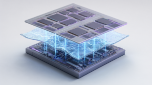
The significance of packaging technology in semiconductor manufacturing has dramatically increased, with pitch miniaturization, often termed “vertical competition,” becoming crucial for enhancing next-generation chip performance and cost efficiency. Within this context, copper-to-copper hybrid bonding is positioned as a major technological breakthrough, enabling higher-density interconnects that surpass the capabilities of traditional microbump technologies.
Technical Details
Copper-to-copper hybrid bonding facilitates direct die-to-die or wafer-to-wafer connections, offering finer pitches (sub-micron level), superior electrical performance, and better thermal conductivity compared to conventional solder microbumps. This technology necessitates extremely high demands for connection density, concomitant surface quality, and assembly precision. The article emphasizes that the ability to co-design interposers, optimize bonding processes, establish effective thermal pathways, and implement precise inspection as a single, integrated yield learning system is paramount. This integrated approach enhances coordination between stages, maximizing overall manufacturing yield and reliability.
Background & Context
As the limits of Moore’s Law draw near, achieving performance improvements solely through transistor scaling is becoming increasingly difficult and costly. In response, packaging technologies, particularly 3D stacking and heterogeneous integration using chiplets, have emerged as a new frontier for enhancing semiconductor performance. Copper-to-copper hybrid bonding is central to this new paradigm, becoming indispensable for supporting the evolution of AI, high-performance computing, and mobile applications.
Strategic Significance & Outlook
Copper-to-copper hybrid bonding will remain a critical technology for shaping the future of high-density packaging. Its further proliferation and evolution depend on the integrated co-design capabilities of the entire ecosystem, including interposers, bonding equipment, thermal management solutions, and inspection systems. Such an integrated approach will provide semiconductor manufacturers with a sustainable competitive advantage and accelerate the realization of next-generation AI chips and high-performance devices.
Source: https://www.geninnov.ai/blog/the-real-loops-of-innovation
Get our weekly technology intelligence — free
Receive an infographic that lets you judge at a glance whether each field’s analysis report is worth reading.
Subscribe Free — Weekly Tech Intelligence
By subscribing, you’ll receive Troy-Technical’s weekly technology intelligence newsletter.
- Your email and selected fields are used only to deliver the newsletter.
- We never share your information with third parties.
- You can unsubscribe anytime via the link in each email.
See our Privacy Policy for details.
Takes about a minute · Unsubscribe anytime