TECHNOLOGY EXPLAINER
What a Bump Is
— tens of thousands of tiny pillars standing under the chip
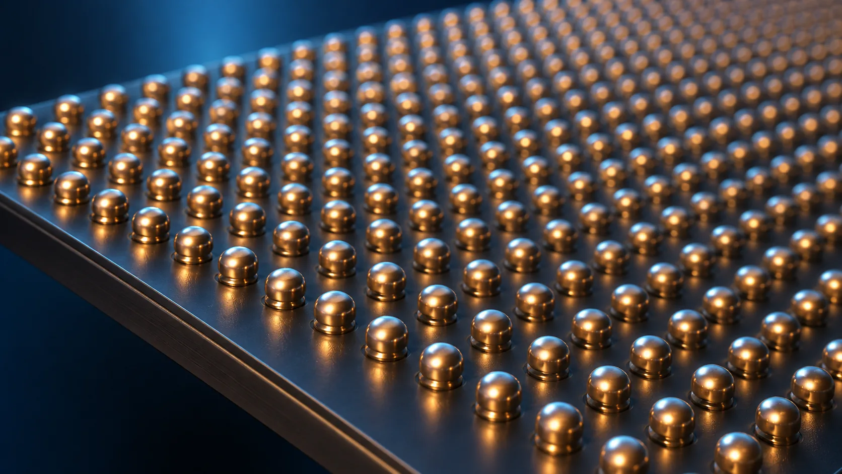
When a chip is flipped over and joined to a substrate, the small protrusions standing between the two are bumps. They look like nothing more than beads of metal, but inside they are a stack of several different metals, and reactions keep running inside them long after the joint is made. Of everything in the back end, a bump is where materials design itself most directly sets product performance.
- What a bump is (the short version)
- Why bumps are needed — from the edge to the face
- A bump in cross-section — the invisible layer called UBM
- How bumps are made — three processes
- A materials engineer's view 1: UBM is a layer for stopping things
- From solder bumps to copper pillars
- A materials engineer's view 2: left alone, a joint turns into intermetallic
- What is still hard
- Glossary / Primary sources / Claim-to-source audit
Sourced = content stated in a company's published material or a technical paper (link given)
Our calculation = a figure this article derived, with the assumptions spelled out
Not yet confirmed = a plan with no confirmed track record
Beyond those, structural framing and readings about materials design are marked Commentary.
1. What a bump is (the short version)
A bump is a small protrusion formed on top of a chip electrode, there to make a connection. In describing its wafer post-processing service, Kyocera calls it the step that "forms solder bumps (protrusions) on the electrode areas of a semiconductor wafer"Sourced.
- What it is for: flipping the chip over (flip chip) and joining it face-to-face with a substrate or another chip
- What it is made of: solder, or a copper pillar with a solder cap. And always, underneath, a foundation layer called UBM
- Where it is made: at the entrance to the back end, while still a wafer, before anything is cut
In a photograph, bumps look like beads of metal in rows and nothing more. In fact, several invisibly thin layers are laid down beneath each bead. Without knowing that foundation — it is called UBM — you cannot follow half of what is said about bumps. Just as with wire materials in the Bonding article, the lead role here belongs to the choice of layer materials.
2. Why bumps are needed — from the edge to the face
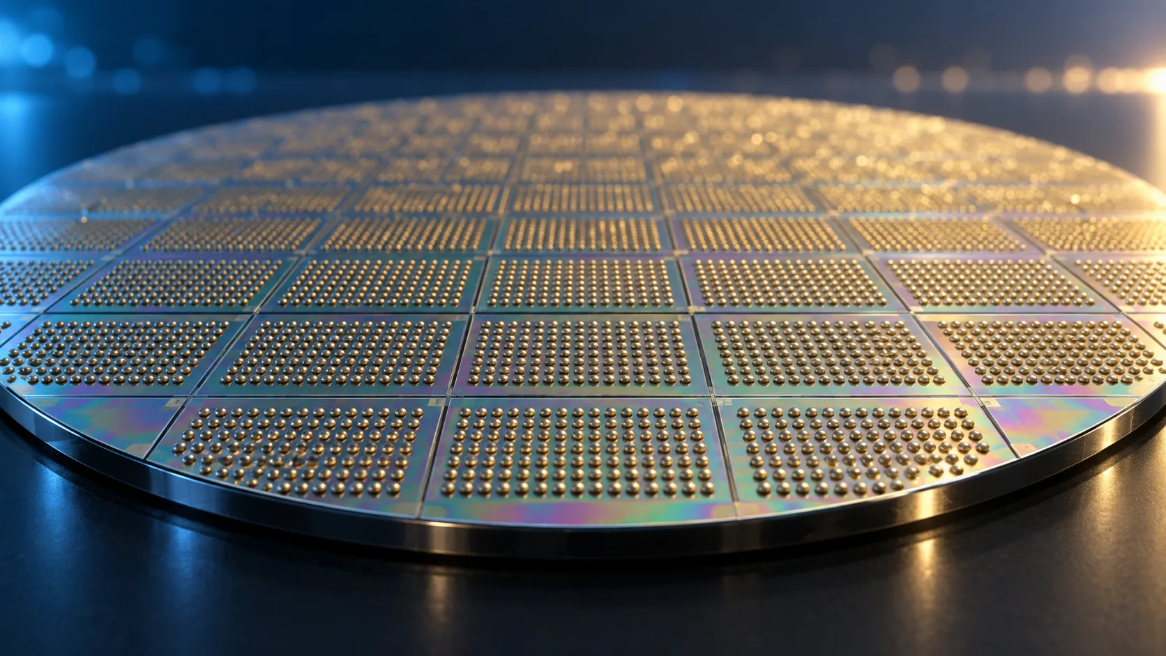
As the Bonding article noted, wire bonding can only bring terminals out at the edge of a chip. Bumps make the whole underside available. Here is what that difference is worth, in numbers.
Does terminal count scale with the length of the edge, or with the area? That difference bites harder the larger the chip gets. For a device needing thousands to tens of thousands of terminals, such as HBM or an AI accelerator, there is no option but bumps (Commentary).
3. A bump in cross-section — the invisible layer called UBM
Cut a bump open and look at the section, and beneath the solder on top there are several thin layers of metal. That is UBM. Kyocera gives UBM as "short for either under barrier metal or under bump metal", and describes it as carrying "the role of improving the solder joinability between the electrode pad and the electrode on the substrate side" of a semiconductor deviceSourced.
4. How bumps are made — three processes
Kyocera sorts solder bump processing into three methodsSourced. What is interesting is that the three divide not by which is better but by which size each is good at.
Plating is good "below about 50 µm in height", because "forming a large bump size requires an enormous plating time"Sourced. Ball mount covers "about 100 µm in height and above", printing "about 50 to 100 µm in height"Sourced.
So the three processes map straight onto three size bands. Seen from the materials side, that means the same solder comes in three supply forms: a plating bath, a ball, a paste. The same alloy composition becomes an entirely different product depending on whether it is sold as a liquid, a sphere or a paste (Commentary).
5. A materials engineer's view 1: UBM is a layer for stopping things
Kyocera sorts UBM formation into five methods as wellSourced. And again, the difference between methods is a difference in the thickness each can make.
What is UBM stopping?
The name UBM is also read as under barrier metalSourced. Barrier — that is, a layer that stops something. Stops what?
The main constituent of solder is Sn (tin). Sn reacts eagerly with whatever metal is beneath it. Left alone it eats through the electrode pad and reaches the wiring underneath. So UBM is built as a stack of a layer the solder wets happily and a layer that will not let that reaction go any deeper.
Kyocera's Ni-based electroless UBM plating comes in three kinds: Ni/Au, Ni/thick Au and Ni/Pd/AuSourced. By the company's account, for semiconductor device electrodes "Ni (nickel) has good affinity with Al (aluminium) based materials", while Au carries both "the role of improving the solder joinability between the semiconductor device electrode and the substrate-side electrode" and "the role of protecting the electrode"Sourced.
Kyocera explains Ni/Pd/Au plating this way. Because "in a high-temperature environment, a phenomenon can occur in which the underlying Ni diffuses to the surface of the Au plating", the company adopts "Ni/Pd/Au plating, with Pd (palladium) inserted as an intermediate layer to suppress Ni diffusion"Sourced.
Put another way, what is happening is this.
- You want Au on the surface, to prevent oxidation and make the solder wet well
- But an Au film always has pinholes
- Get it hot and the Ni underneath climbs up through them and reaches the surface
- Once Ni is on the surface, there was no point putting the Au there at all
- So between Au and Ni you insert one layer of a metal Ni finds hard to cross (Pd)
Pd is not performing any function of its own. It is there solely to get in the way of Ni moving. Recall the Bonding article, where Pd was coated over copper wire to stop it oxidising. In this field Pd turns up again and again in the role of stopping diffusion (Commentary).
One more thing. Kyocera also lists "increasing the thickness of the Au plating" as a remedySourced. Thicken it so pinholes are less likely to go all the way through, or plug them with a different metal — both are textbook answers to pinholes in a thin film. The first spends extra precious metal; the second adds a process step. Which one you pick is a question of cost and step count, not of performance (Commentary).
On missing or chipped UBM, Kyocera states that "an electrode terminal on which UBM has not formed has poor solder wettability and causes solder joint defects when the semiconductor device is mounted"Sourced. The cause is given as contamination on the electrode terminal surface, and the remedy as adding an ashing step or optimising the wafer cleaning stepSourced.
UBM is a layer a few micrometres thick at most. Simply because it is absent, neither the bump placed on top nor the assembly beyond it can succeed. The rule of thumb that back-end trouble usually traces back to a dirty interface holds here too (Commentary).
6. From solder bumps to copper pillars
Keep making bumps smaller and the solder itself becomes the obstacle, because solder spreads sideways when you squash it. Touch a neighbour and you have a short.
Which is where the copper pillar came in: instead of a bead of solder, a copper post is stood up with a solder cap on its tip alone.
Amkor positions the copper pillar as "next generation bump technology for greater density, reliability and performance", "fine pitch capable down to 30 µm in-line and 30/60 µm staggered", and for TSV and chip-on-chip silicon packages, "extreme fine pitch on silicon package down to 30 µm"Sourced.
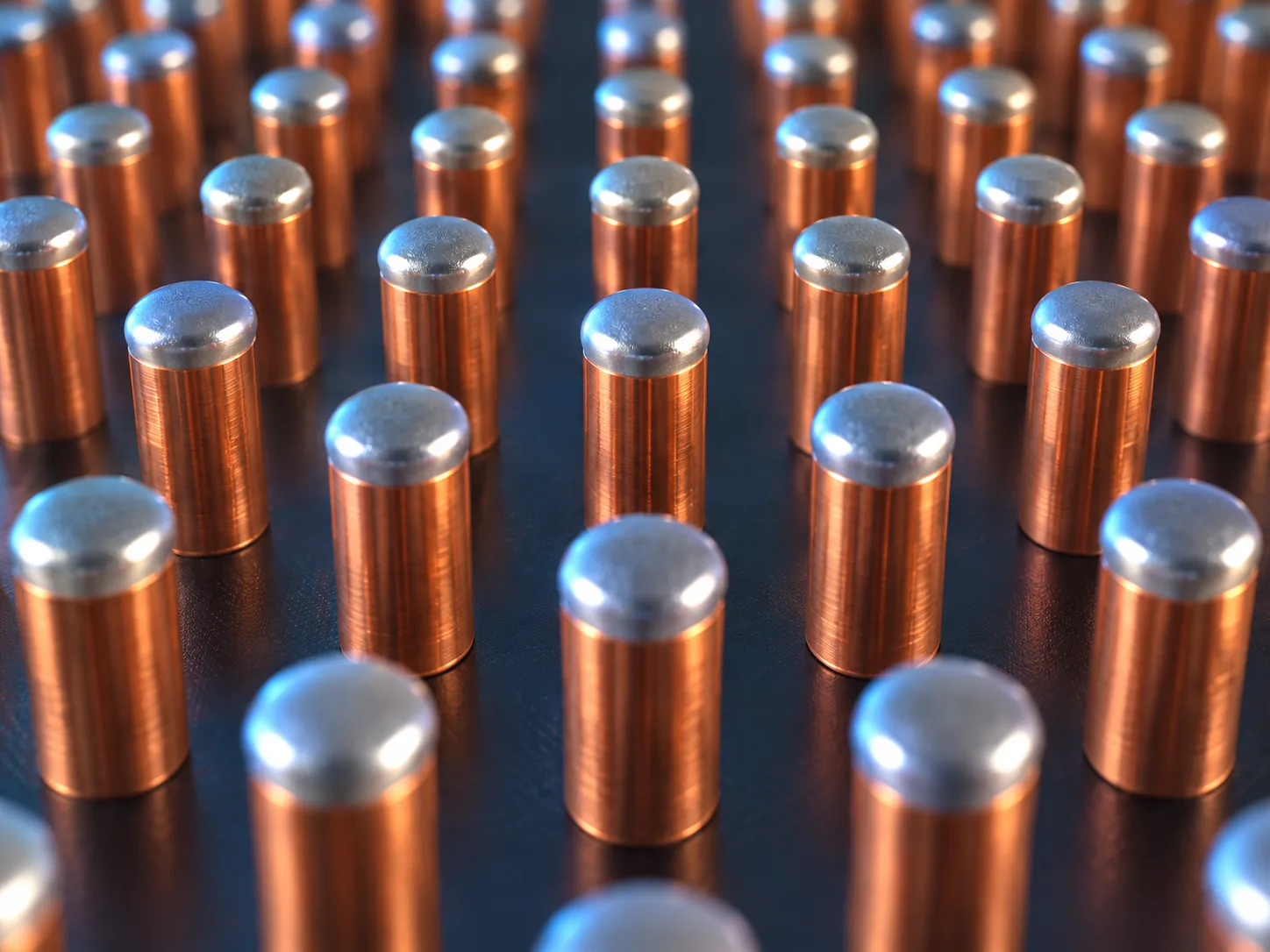
Amkor lists among the advantages of copper pillars "superior electromigration performance for high-current carrying capacity"Sourced.
This is the point at which it stops being about shape and becomes about materials. In a solder bump, current runs through solder from one end to the other. In a copper pillar, current runs mostly through copper, with solder only as a thin layer at the tip.
Electromigration (EM) is the phenomenon of metal atoms being swept along by current. The narrower the path and the larger the current, the more readily it happens. Shorten the distance the current travels through solder and you shorten the stretch that is weak to EM — that is the materials-side account of why copper pillars resist EM (Commentary).
The layer stacks Amkor publishes are worth noticing too: "Cu+Ni+Pb-free, Cu+Ni+Cu+Pb-free"Sourced. There is Ni sandwiched between the copper post and the solder cap. The same job as the UBM in the previous section. Ni is there to stop Sn eating its way into the copper (Commentary).
7. A materials engineer's view 2: left alone, a joint turns into intermetallic
This is the most important part of the article. A solder joint is not finished at the instant it sticks.
On cross-sections of solder joint interfaces, JFE Techno-Research reports seeing, in order from the top, "Sn in the solder, then the intermetallic compounds Cu6Sn5 and Cu3Sn produced by interdiffusion between the Sn in the solder and the Cu of the printed board wiring"Sourced.
As long as they are in contact, Sn and Cu keep reacting according to time and temperature. What that produces is intermetallic compound (IMC). And here is the frightening part: cavities form inside it.
The smaller the bump, the more this matters
If the joint is large, a few micrometres of intermetallic at the interface is a skin on the whole thing. But as bumps shrink, that skin comes to occupy most of the joint.
Work by Seongcheol Jeong, Yuki Sato and Hideo Miura at Tohoku University finds that the volume fraction of intermetallic "increases sharply as bumps are made finer", raising the concern that this "will substantially change the characteristics of fine bump connections"Sourced.
What this calculation shows is not merely that a fraction goes up.
Solder is soft, and relieves stress by deforming. Intermetallic is hard and brittle. For most of the joint to become intermetallic means a soft joint turning into a hard, brittle one.
Which is to say that on fine bumps, the whole design philosophy of solder joining stops applying. The move to direct Cu-to-Cu bonding (hybrid bonding) seen in the Bonding article is not driven by equipment progress alone. Go small enough and the premise of using solder at all falls apart — that is the materials-side reason for the transition (Commentary).
8. What is still hard
(1) How closely can you match the amount of solder?
Senju Metal Industry describes its solder balls as "a product with very high stability of solder volume, through excellent sphericity and strict dimensional control"Sourced. Why is sphericity stressed that heavily? The reason is volume.
The volume of a sphere goes as the cube of its diameter. So Our calculation:
- A 1% error in diameter gives roughly a 3.0% error in solder volume (1.01³ = about 1.030)
- A 3% error in diameter gives roughly a 9.3% error (1.03³ = about 1.093)
- A 5% error in diameter gives roughly a 15.8% error (1.05³ = about 1.158)
Assumption: a simple calculation treating the ball as a perfect sphere. In reality departure from sphericity, surface oxide and spreading during reflow all count, so the volume does not come out exactly like this.
The meaning is clear all the same. A slight spread in diameter shows up amplified threefold in solder volume. Vary the solder volume and the post-join height (standoff) varies with it; stress concentrates on the low bumps, and the over-full ones spread sideways and touch their neighbours. Sphericity and strict dimensional control are selling points precisely because of that cube law (Commentary).
(2) Alpha particles — the radiation solder emits
This is a fairly unusual problem to have with a material. Senju Metal Industry explains it as followsSourced.
"Soft errors, in which data in memory is rewritten by trace alpha particles emitted from solder or semiconductor materials, or by cosmic rays. Flip chip packages in particular are highly sensitive to soft errors, and low alpha emission is therefore demanded of mounting materials such as solder. LAS (low alpha solder) was developed to satisfy these requirements."
In a wire-bonded package the solder sits some distance from the chip. In flip chip it does not. The bump is attached directly to the circuit face of the chip.
Hence the company's line that "flip chip packages in particular are highly sensitive to soft errors"Sourced. A change in mounting method has changed what purity means for the material.
The difficulty of materials development is concentrated in this example. Performance as a solder is to stay exactly the same; only the radioactive impurities are to go down. You cannot differentiate on performance, yet it is hard to make. The value of a product like that is set not by the spec table but by the ability to control impurities (Commentary).
(3) Do not confuse the two kinds of migration
Two very similar words turn up in the literature on bumps.
| Term | What happens | Conditions that drive it | Where it appears in this article |
|---|---|---|---|
| Electromigration (EM) | Large current sweeps metal atoms along, opening cavities and raising hillocks | High current density. No moisture needed | Amkor cites "superior electromigration performance" as an advantage of copper pillars |
| Electrochemical migration (ECM) | Metal moves as ions and grows dendrites that bridge to the neighbour | Moisture and a potential difference. The narrower the gap, the easier | Senju Metal Industry describes its Cu core balls as having "excellent resistance to electrochemical migration" |
The companies' wording (right column) follows their published material [Sources 6 and 7]. The account of what each phenomenon is and what drives it (the middle two columns) is this article's own framing, not a statement by either company.
Both are called migration, but the cause and the conditions are different things. EM is a question of how much current; ECM a question of moisture and spacing. Make bumps finer and the cross-section of each shrinks, so EM gets worse, while the gap to the neighbour narrows, so ECM gets worse too — scaling degrades both at the same time (Commentary).
Read in that context, Senju Metal Industry's Cu core ball makes obvious sense. The company describes it as "a ball of solder plating over a copper core. It secures an appropriate gap at the moment of joining, offers excellent resistance to electrochemical migration in fine-pitch mounting, and contributes to better heat dissipation"Sourced. Put a copper core inside that will not squash, and a set height survives however hard you press. The thinking is the same as the copper pillar. Not relying on solder alone is emerging from the sphere side as well as the post side (Commentary).
(4) Can the process keep up?
Bump pitch keeps shrinking. Amkor reaches 30 µm with copper pillarsSourced, and Kulicke & Soffa gives thermocompression bonding as "down to 10 µm pitch" for solder-based joining and "down to at least 5 µm pitch" for direct copper-to-copperSourced.
Look at the bump-forming side, meanwhile, and even plating, the finest-capable of Kyocera's three processes, is at its best "below about 50 µm in height"Sourced. Height and pitch are different dimensions, but it is certainly true that the forming side and the joining side are both continuing to get finer at once (Commentary).
Of everything in the back end, a bump is particularly a technology of layers and of time.
- Layers: all you see is the protrusion, but UBM sits underneath, and that UBM itself divides into adhesion, barrier, wetting and protection
- Time: the moment of joining is not completion. Intermetallic grows at the interface, and cavities grow inside it
- Size: go smaller and the intermetallic fraction leaps, changing the nature of the joint itself
- Purity: because it now sits directly over the chip, even the radioactive impurities in solder became something to control
And materials whose job is to stop things are inserted all over it. Ti and TiW stop Sn getting in, Ni stops the attack on Cu, Pd stops Ni diffusing. A bump cross-section can be read as a list of things somebody wanted to stop (Commentary).
9. Glossary
- Bump
- A protrusion made on a chip electrode to carry a connection. Built from solder, or a copper post plus solder.
- UBM
- Under bump metal, or under barrier metal. The foundation metal layers placed between bump and electrode pad.
- Passivation film
- The protective film covering the chip surface, opened only over the electrodes.
- Electroplating
- Plating driven by electrical energy from an external supply. Can build thick layers.
- Electroless plating
- Plating driven by the difference in metal ionisation energy. No external supply needed.
- Dry plating
- The collective term for vacuum evaporation, sputtering and CVD. Suited to layers on the order of nanometres.
- Reflow
- The step of heating to melt solder, shaping it or making the joint.
- Flip chip
- Mounting in which the chip is turned face down and connected to the substrate by bumps across its face.
- Copper pillar
- A bump with solder on the tip of a copper post. Suited to fine pitch and high current.
- Standoff
- The height of the gap left between chip and substrate after joining.
- Intermetallic compound (IMC)
- A compound formed when two or more metals bond in fixed proportions. Hard and brittle.
- Cu6Sn5 and Cu3Sn
- The characteristic intermetallics at a Cu-Sn interface: Cu6Sn5 on the solder side, Cu3Sn on the Cu side.
- Kirkendall void
- A cavity created by the difference in diffusion rate between two interdiffusing metals. Grows into a crack.
- Interdiffusion
- The phenomenon of atoms from two materials in contact moving into one another.
- Electromigration
- Metal atoms moved by a large current, producing open circuits or hillocks.
- Electrochemical migration
- Metal moving as ions under moisture and a potential difference, bridging to the neighbouring conductor.
- Sphericity
- A measure of how accurately a sphere is spherical. Feeds straight into stability of solder volume.
- Solder ball
- A sphere of solder alloy used to form bumps.
- Cu core ball
- A ball with a copper sphere as its core, solder plated over the surface. Holds a gap without squashing.
- Low alpha solder (LAS)
- Solder with reduced radioactive impurities that emit alpha particles. Used against soft errors.
- Soft error
- A transient malfunction in which radiation rewrites data in memory. The device itself is not damaged.
- Staggered layout
- Terminals offset in alternating rows so the effective spacing between them is larger.
10. Primary sources
- Kyocera "Three solder bump processes for semiconductors" (Japanese-language page) — kyocera.co.jp
- Kyocera "Five UBM plating methods" (Japanese-language page) — kyocera.co.jp
- Kyocera "How electroless UBM plating defects affect semiconductor device mounting: non-deposition, chipping and Ni diffusion" (Japanese-language page) — kyocera.co.jp
- Kyocera "Ni-based electroless UBM plating, combining high reliability with short lead times" (Japanese-language page) — kyocera.co.jp
- Kyocera "What is Kyocera's own hybrid printing method? Solder bump processing for semiconductors" (Japanese-language page) — kyocera.co.jp
- Amkor "Copper Pillar (Cu Pillar)" — amkor.com
- Senju Metal Industry "Solder balls" (Japanese-language page) — senju.com
- JFE Techno-Research "Observation of intermetallic compound layers at solder joint interfaces" (JFE-TEC News) (Japanese-language page) — jfe-tec.co.jp
- Seongcheol Jeong, Yuki Sato and Hideo Miura (Tohoku University) "A study of the influence of intermetallic compounds on the electrical and mechanical reliability of lead-free fine bump connections", Proceedings of the 23rd Symposium on Microjoining and Assembly Technology in Electronics (2009) (Japanese-language page) — jstage.jst.go.jp
- Kulicke & Soffa "Thermo-Compression Bonding" — kns.com
11. Claim-to-source audit
| Claim in the text | Basis | Label |
|---|---|---|
| That bump formation is the step that "forms solder bumps (protrusions) on the electrode areas of a semiconductor wafer"; and the content of the three processes: plated bumps (electroplated solder, resist strip, seed etch, then reflow to shape the bump; best below about 50 µm in height; large bumps need enormous plating time; photoresist patterning required), ball mount (solder balls dropped into the openings of a metal mask; best at about 100 µm and above; consistent bump size; a missed ball must be remounted) and screen printing (paste pressed through with a squeegee; best at about 50 to 100 µm; short lead time; few process steps) | Kyocera "Three solder bump processes for semiconductors"[Source 1] https://www.kyocera.co.jp/prdct/wafer-bumping/howto_wbp/bumping/ | Sourced |
| That UBM is "short for either under barrier metal or under bump metal" and carries "the role of improving the solder joinability between the electrode pad and the electrode on the substrate side"; that electroplating is "driven by electrical energy from an external supply" and forms "UBM layers of tens of µm and above"; that electroless plating is driven by the difference in metal ionisation energy, needs no external supply and can run many wafers at once, reaching a few µm; and that dry plating (vacuum evaporation, sputtering, CVD) forms layers on the order of nanometres, needs a mask, and in the CVD case wraps around step corners and curved surfaces | Kyocera "Five UBM plating methods"[Source 2] https://www.kyocera.co.jp/prdct/wafer-bumping/howto_wbp/ubm_type/ | Sourced |
| That "an electrode terminal on which UBM has not formed has poor solder wettability and causes solder joint defects when the semiconductor device is mounted"; that the cause is contamination on the electrode terminal surface and the remedy is adding an ashing step or optimising wafer cleaning; and that "in a high-temperature environment, a phenomenon can occur in which the underlying Ni diffuses to the surface of the Au plating", so that "the high corrosion resistance which is the purpose of the Au plating is impaired", with remedies of thickening the Au or inserting Pd | Kyocera "How electroless UBM plating defects affect semiconductor device mounting"[Source 3] https://www.kyocera.co.jp/prdct/wafer-bumping/howto_wbp/ubm_process/ | Sourced |
| That Ni-based electroless UBM plating comes in three kinds, Ni/Au, Ni/thick Au and Ni/Pd/Au; that there is a description of "Ni/thick Au plating, with the Au plating layer secured at 0.1 µm or more"; that "Ni (nickel) has good affinity with Al (aluminium) based materials"; and that Au carries both the role of improving solder joinability and the role of protecting the electrode | Kyocera "Ni-based electroless UBM plating"[Source 4] https://www.kyocera.co.jp/prdct/wafer-bumping/howto_wbp/ni_plating/ | Sourced |
| That Kyocera's own hybrid printing method delivers "stable solder bump processing accuracy at a bump pitch of 100 µm" | Kyocera "Hybrid printing method"[Source 5] https://www.kyocera.co.jp/prdct/wafer-bumping/howto_wbp/hybrid_printing/ | Sourced |
| That the copper pillar is "next generation bump technology for greater density, reliability and performance"; that it is "fine pitch capable down to 30 µm in-line and 30/60 µm staggered" and offers "extreme fine pitch on silicon package down to 30 µm for TSV and CoC"; that it has "superior electromigration performance for high-current carrying capacity"; and that the layer stacks are "Cu+Ni+Pb-free, Cu+Ni+Cu+Pb-free" | Amkor "Copper Pillar"[Source 6] https://amkor.com/technology/copper-pillar/ | Sourced |
| That solder balls are "a product with very high stability of solder volume, through excellent sphericity and strict dimensional control"; that the Cu core ball is "a ball of solder plating over a copper core" which "secures an appropriate gap at the moment of joining, offers excellent resistance to electrochemical migration in fine-pitch mounting, and contributes to better heat dissipation"; and the description of soft errors and of LAS (low alpha solder) | Senju Metal Industry "Solder balls"[Source 7] https://www.senju.com/ja/products/soldering_materials/solder_ball/ | Sourced |
| That a solder joint interface shows, "in order from the top, Sn in the solder, then the intermetallic compounds Cu6Sn5 and Cu3Sn produced by interdiffusion between the Sn in the solder and the Cu of the printed board wiring"; that the Cu3Sn layer develops "Kirkendall voids arising from the difference in atomic diffusion rates"; and that "when these Kirkendall voids grow they develop into cracks, the solder joint is destroyed, and this can become a cause of failure" | JFE Techno-Research "Observation of intermetallic compound layers at solder joint interfaces"[Source 8] https://www.jfe-tec.co.jp/jfetec-news/k_news/46.html | Sourced |
| That the volume fraction of intermetallic "increases sharply as bumps are made finer", and that this "raises the concern that it will substantially change the characteristics of fine bump connections" (authors: Seongcheol Jeong, Yuki Sato and Hideo Miura, Tohoku University, 2009) | Jeong, Sato and Miura, Tohoku University (2009)[Source 9] https://www.jstage.jst.go.jp/article/ejisso/23/0/23_170/_article/-char/ja/ | Sourced |
| That the pitch thermocompression bonding supports is "down to 10 µm pitch" on a solder base and "down to at least 5 µm pitch" for Cu-to-Cu | Kulicke & Soffa "Thermo-Compression Bonding"[Source 10] https://www.kns.com/products-services/thermo-compression-bonding | Sourced |
| Fig. 1: with L the chip side length and p the terminal pitch, 4 × (L/p) terminals on a perimeter layout and (L/p)² on an area layout; 400 against 10,000 terminals, a factor of 25, at L = 10 mm and p = 100 µm | Our calculation. It does not include constraints such as power and ground placement, keep-out zones or the number of routable layers on the substrate | Our calculation |
| Fig. 10: for a joint height h, the intermetallic volume fraction taken as 2/h assuming 2 µm of total intermetallic across the two interfaces (100 µm gives 4%, 50 µm 8%, 20 µm 20%, 10 µm 40%, 5 µm 80%) | Our calculation. The 2 µm is this article's assumption; real thickness varies with temperature, time and material system. The qualitative trend follows Source 9[Source 9] https://www.jstage.jst.go.jp/article/ejisso/23/0/23_170/_article/-char/ja/ | Our calculation |
| That because sphere volume goes as the cube of diameter, errors of 1%, 3% and 5% in diameter give roughly 3.0%, 9.3% and 15.8% errors in solder volume | Our calculation, treating the ball as a perfect sphere. Departure from sphericity, surface oxide and spreading during reflow are not included. The context of sphericity comes from Source 7[Source 7] https://www.senju.com/ja/products/soldering_materials/solder_ball/ | Our calculation |
| The account of what electromigration and electrochemical migration are and of the conditions that drive them (the middle two columns of the table) | Commentary by this article. A general description of the two phenomena, not something stated by the companies in Sources 6 and 7, whose own wording is reproduced in the right-hand column | Commentary |
| The framing of UBM as three layers (adhesion/barrier, wetting, protection); the reading that UBM is a layer stopping Sn getting in; the reading that Pd is there solely to get in the way of Ni moving; the explanation of copper pillar EM resistance as shortening the distance current travels in solder; the reading that intermetallic fraction changes the nature of the joint and so underlies the move to Cu-to-Cu bonding; and the point that the same solder becomes a different product as bath, ball or paste | Commentary and framing by this article, built on published material. Not a view expressed by any of the companies, nor an established industry classification | Commentary |
| That the cross-sections in Figs. 3, 6 and 9 are drawings for explanation rather than observed images such as photographs or SEM images | Our note in this article | Commentary |
Last updated 20 September 2026. Sources are limited to primary material (official technical pages from materials makers, contract processing houses and package makers, a technical article from an analysis services company, and a peer-reviewed conference paper). Because the article contains structural framing and readings about materials design, those passages are marked Commentary to separate them from sourced fact. All figures are explanatory concept graphics. Visual-overview figures are shown as AI-generated conceptual images, matching the Japanese edition. Vector drawings are retained where they carry quantitative values or precision-critical technical labels. AI-generated images do not depict real equipment, products, facilities, dimensions or exact cross-sections; replaced source SVG overview drawings remain in the HTML but are hidden.