TECHNOLOGY EXPLAINER
What Bonding Is
— heat, pressure and ultrasound, for sticking metal to metal
A semiconductor package is a set of separate parts wired electrically together. Making those joins is bonding. From wire bonding, in service for more than sixty years, to the newest joining aimed at 5 µm pitch, this step is made, throughout, of choices about materials.
- What bonding is (the short version)
- Why sticking things together is hard
- A map of joining — what is joined where in a package, and with what
- Wire bonding — a technology still in use after sixty years
- A materials engineer's view 1: from gold to copper, and on to silver
- Flip chip and TCB — turn it over and join across the face
- A materials engineer's view 2: die bonding is a contest between a film and a powder
- What is still hard
- Glossary / Primary sources / Claim-to-source audit
Sourced = content stated in a company's published material (link given)
Our calculation = a figure this article derived, with the assumptions spelled out
Not yet confirmed = a plan with no confirmed track record
Beyond those, process framing and readings about materials design are marked Commentary.
1. What bonding is (the short version)
Bonding is the step that joins separately made parts together in a state where current can flow. Boiled down, the semiconductor back end is that operation repeated.
- What gets joined: chip to substrate, chip to chip, chip to lead frame, package to motherboard
- What joins them: a fine metal wire, a bead of solder (a bump), an adhesive film, a metal paste, or direct bonding of the metals themselves
- What does the joining: heat, pressure (load) and ultrasound. Whatever the method, those are broadly the three tools
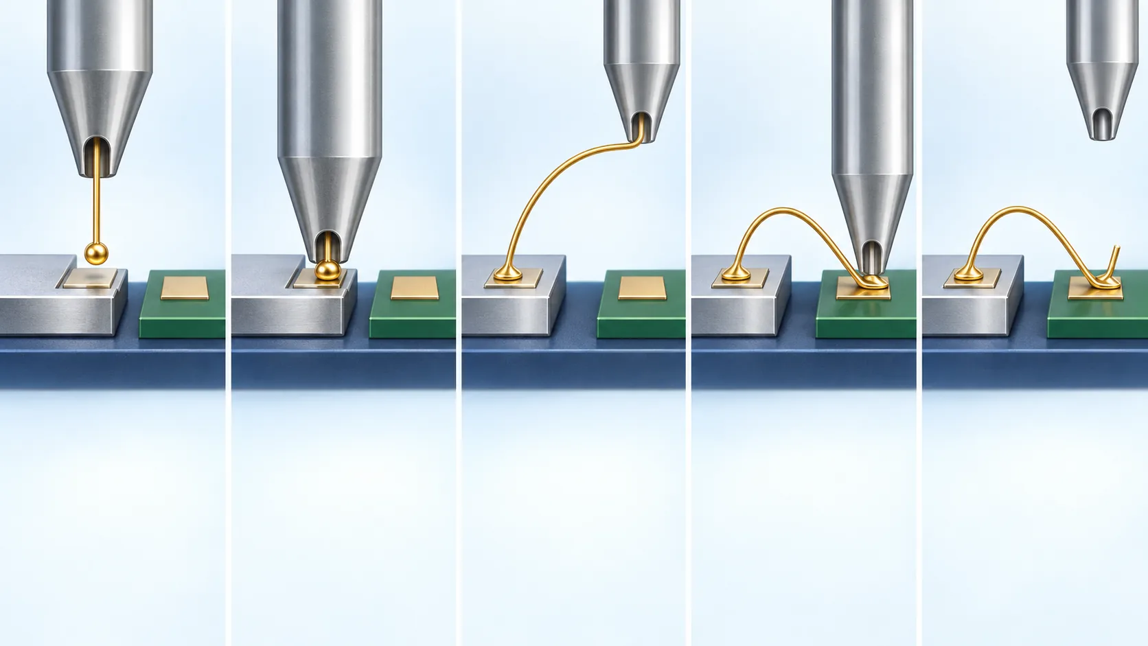
Nippon Micrometal describes bonding wire as "a fine metal wire that carries the electrical signals of a semiconductor element to the outside", and the joining step as "bonding the ball to the semiconductor element using heat, ultrasound and load (the first bond)"Sourced. That set of three, heat, ultrasound and load, is the spine of this article.
Hearing "stick together", you may picture glue or welding. But most semiconductor joining involves no melting at all. Metals are pressed against one another, the dirt and oxide on the surface is broken up, and they are brought close enough for atoms to diffuse across. Joining without melting — that is the first thing to get past.
2. Why sticking things together is hard
Press two clean metals together and in principle they join. In practice they do not. There are three reasons.
(1) The surface is oxidised
Aluminium and copper both grow an oxide the instant they meet air, and oxide is an insulator. Press them together and that film stays trapped in between. (The Test article described a probe needle breaking an oxide; the same problem turns up here.)
(2) The surface is not flat
Under a microscope, any metal surface is rough. Press two together and what actually touches is only the peaks. The contacting area is far smaller than the apparent area.
(3) Semiconductors do not like heat
So melt it at high temperature, then? No. Fine wiring is built into the top of the chip, and organic substrates warp as temperature rises. The temperature needed to make the join and the temperature the parts can survive are always in tension.
The move that solves all three troubles at once is ultrasound.
- Load flattens the roughness and increases the area actually in contact
- Ultrasound scrubs laterally in tiny strokes, cracking the oxide and exposing fresh metal
- Heat makes the atoms mobile, driving diffusion and stabilising the joint
With ultrasound you can join without melting, and at a comparatively low temperature. That is one reason wire bonding has stayed in active service for more than sixty years (Commentary).
3. A map of joining — what is joined where in a package, and with what
The single word "bonding" covers a lot of ground, so let us first sort it by location.
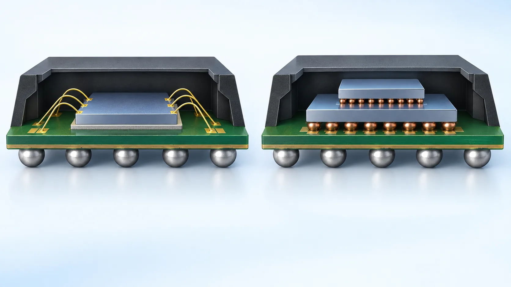
This article works through 1. die bonding, 2. wire bonding and 3. flip chip and die-to-die joining in turn. The leading edge of 3, hybrid bonding (joining Cu directly to Cu without solder), is covered in detail in the separate Hybrid Bonding article.
4. Wire bonding — a technology still in use after sixty years
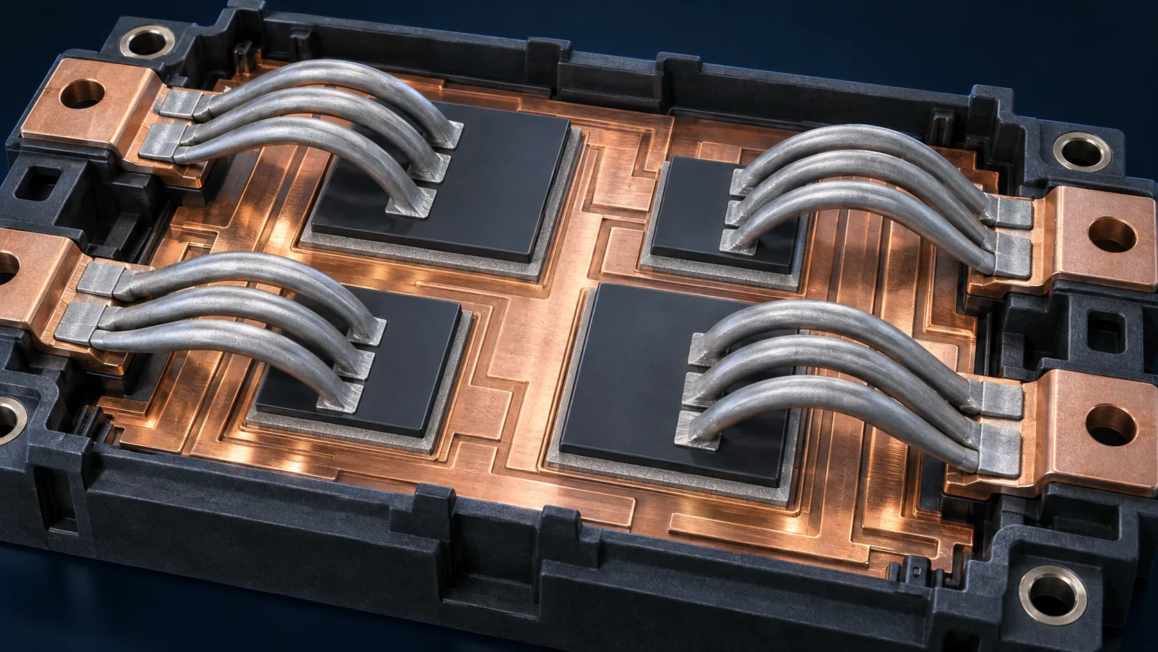
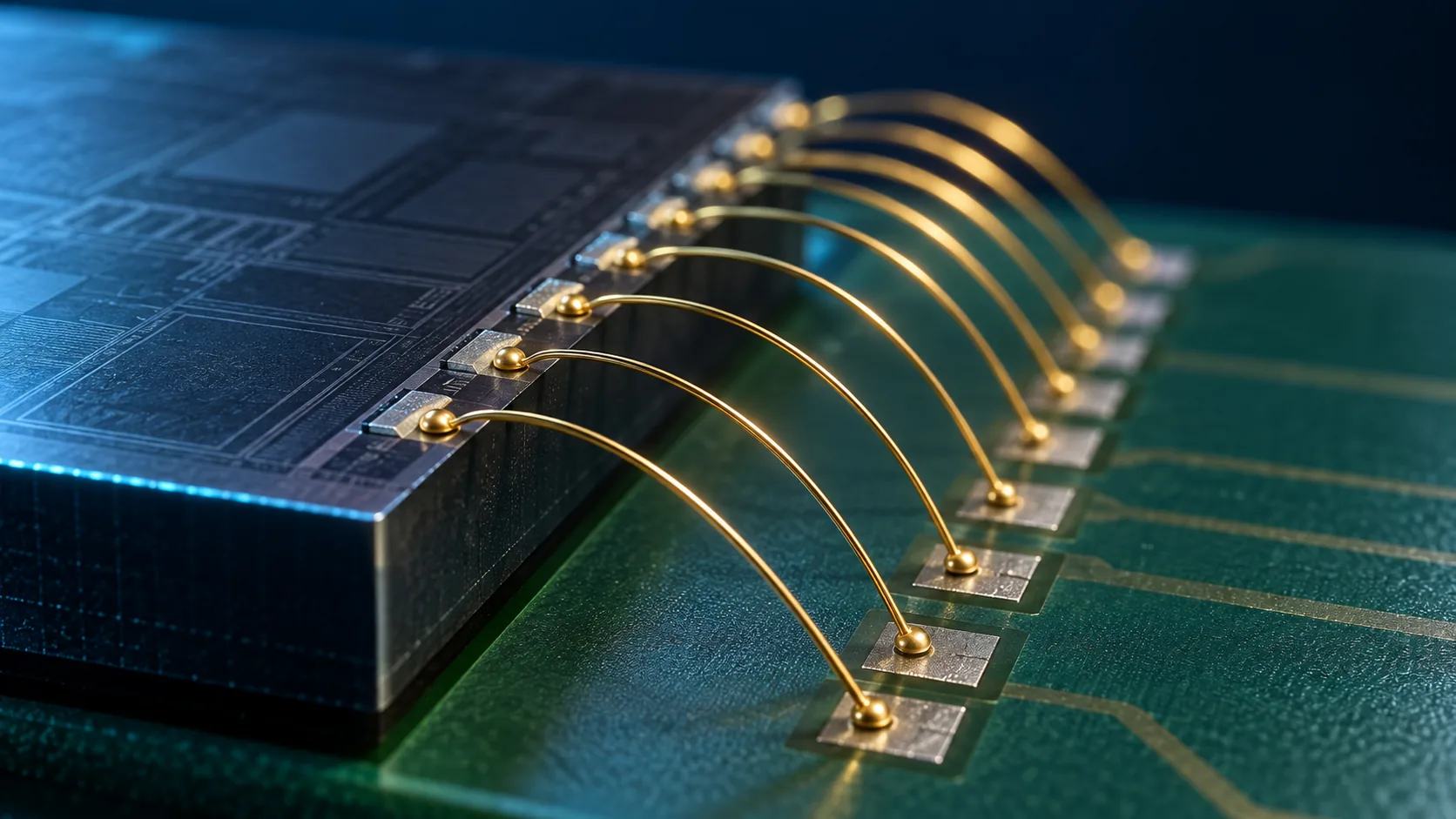
According to Nippon Micrometal, "the wire bonding method of connection was developed in the late 1950s by researchers at Bell Laboratories in the United States"Sourced. It is a technology almost exactly as old as the semiconductor itself.
The wire used runs "from as fine as 15 µm to as thick as around 500 µm". In high-performance packages the wires are "strung at intervals of roughly 30 to 50 µm"Sourced. A human hair is about 80 µm across, so the fine end is about a fifth of a hair.
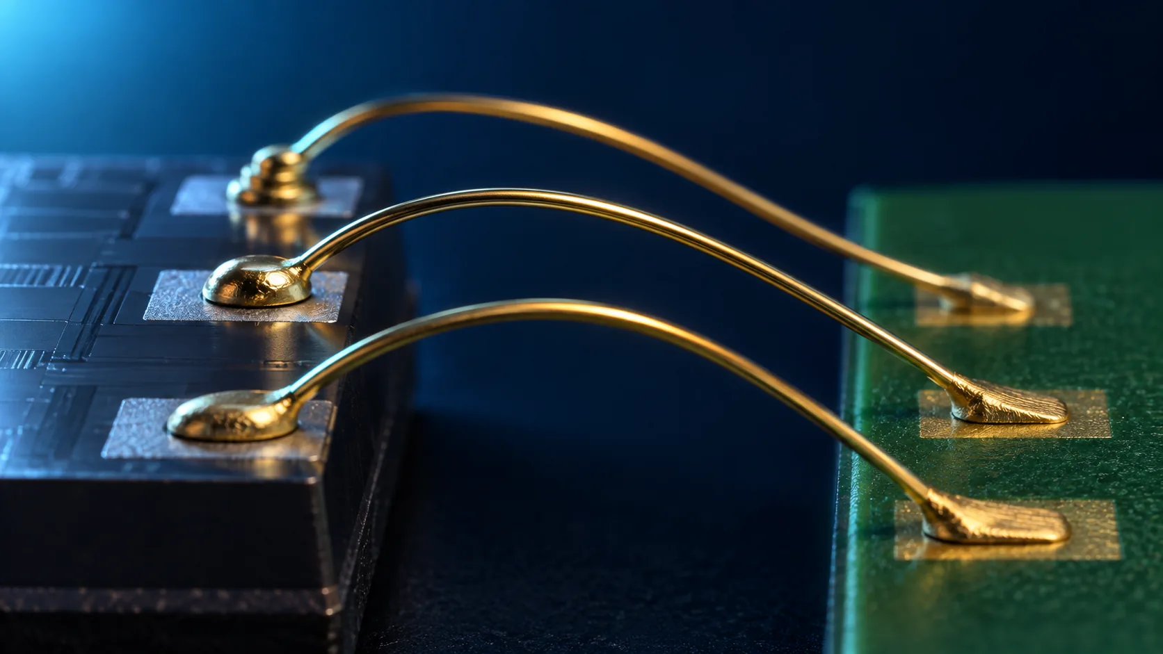
The conditions under which things stick have width
Here an important term appears that you only find in materials suppliers' literature: the process window.
Nippon Micrometal lists "a very wide process window" among the features of its aluminium wire NL1, publishing the evaluation conditions as 300 µm wire diameter, 700 cN bonding force, shear strength > 1250 cN, and squash width < 1.3 times the wire diameterSourced.
What does that mean? It means there is a range in which two conditions are met at the same time: the joint is strong enough, and yet it has not been squashed too far.
When a materials supplier advertises "a wide process window", that is not a claim about absolute performance. It means "it still bonds properly when conditions drift a little".
On a production floor the machine warms up, the capillary wears, the lot changes. Conditions always spread. So you need a window they will not drift out of. This is exactly the same picture as the needle penetration depth in the Test article. Not a single perfect point but how wide you can make the acceptable range is where materials compete (Commentary).
5. A materials engineer's view 1: from gold to copper, and on to silver
Sixty years of wire bonding is also, straightforwardly, a history of replacing the wire material.
(1) Why gold was abandoned
Nippon Micrometal states that "gold, used for bonding wire for fifty years, was high in performance but extremely expensive", citing "the surge in the gold price during the 2000s" as the backgroundSourced.
(2) Why copper was hard
Copper is cheap and conducts well. The reason it could not be used for so long is that it oxidises. The company explains that by "coating palladium at the nanometre level on the outside of a wire only about a fifth the thickness of a human hair (15 to 30 µm), we achieved bondability and corrosion resistance that were impossible with conventional copper wire"Sourced.
The current standard product, EX1p, is a gold and palladium coated copper bonding wire with gold over the top of that, described as having "improved second bond (stitch bond) performance compared with EX1" and "a better Pd distribution in the FAB (free air ball)"Sourced.
The product photograph of EX1p is marked 16 µm diameterSourced. On the surface of a wire that thin, a palladium layer is formed, and over that a gold layer. And the published spool length runs "up to 5000 m", with the coating uniform over that entire lengthSourced. Surface treatment of 5 km of 16 µm wire, held constant to the nanometre — that is what the phrase "bonding wire manufacturing technology" actually refers to (Commentary).
(3) The other option — silver alloy
Alongside the shift to copper, a path through silver alloy wire has also opened. Nippon Micrometal publishes the following comparison of its GX2s against gold wireSourced.
| Property | GX2s (silver alloy) | Au wire (gold) |
|---|---|---|
| Purity | 98% | 99.99% |
| Electrical resistivity (RT) | 2.4 µΩcm | 2.4 µΩcm |
| Looping performance | Equal or better | — |
| FAB hardness | 41 Hv | 43 Hv |
From Nippon Micrometal's GX product page (figures are typical values) [Source 4].
A wire catalogue lists FAB hardness — the hardness of the free air ball made by the electrical discharge. That looks odd, and is in fact the heart of it.
The ball is pressed into the chip electrode. The harder the ball, the more damage the pad and the layers beneath it take. In the Test article, a probe needle that was too hard punched through the pad and wrecked the circuit underneath. Exactly the same thing happens in wire bonding.
Hence the company's line about GX2, that it "has bondability on a par with gold wire and can handle fragile chips"Sourced. And in the numbers, FAB hardness is 41 Hv against gold's 43 Hv, slightly softer, while resistivity is 2.4 µΩcm, the same as goldSourced.
So the pitch for silver alloy wire is not "better than gold". It is the logic of a substitute: "as soft as gold, conducts like gold, and cheaper". When you replace a material, what you have to win on is not performance but equivalence — a basic fact of materials development, showing up unmodified in a product catalogue (Commentary).
(4) Which material goes where
Do you need thin wire or thick wire? Is the chip fragile or robust? Will it live somewhere hot and humid? Different demands, different metal. Wire bonding, a sixty-year-old technology, is still alive not because of the equipment but because the materials side has kept following the demands (Commentary).
6. Flip chip and TCB — turn it over and join across the face
Wire bonding has one constraint it simply cannot get past: wires can only come out around the edge of the chip.
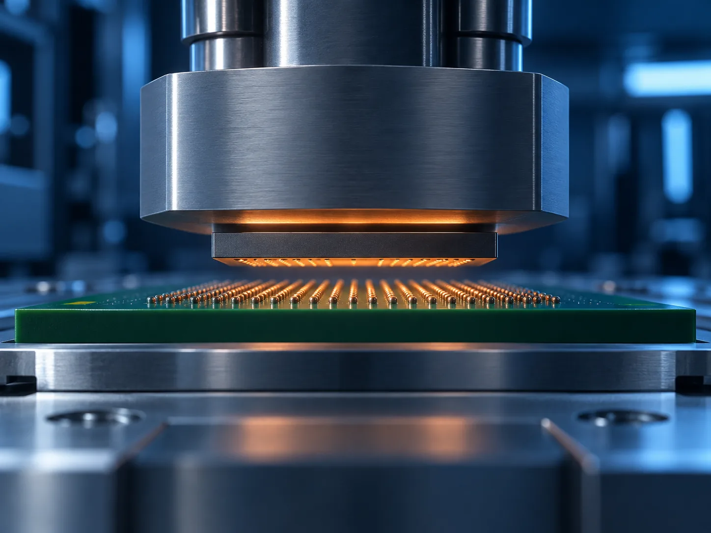
Once a chip grows large and needs thousands or tens of thousands of terminals, the edge is not enough. So the chip is flipped over and connected directly to the substrate by bumps laid across its whole face. That is flip chip joining.
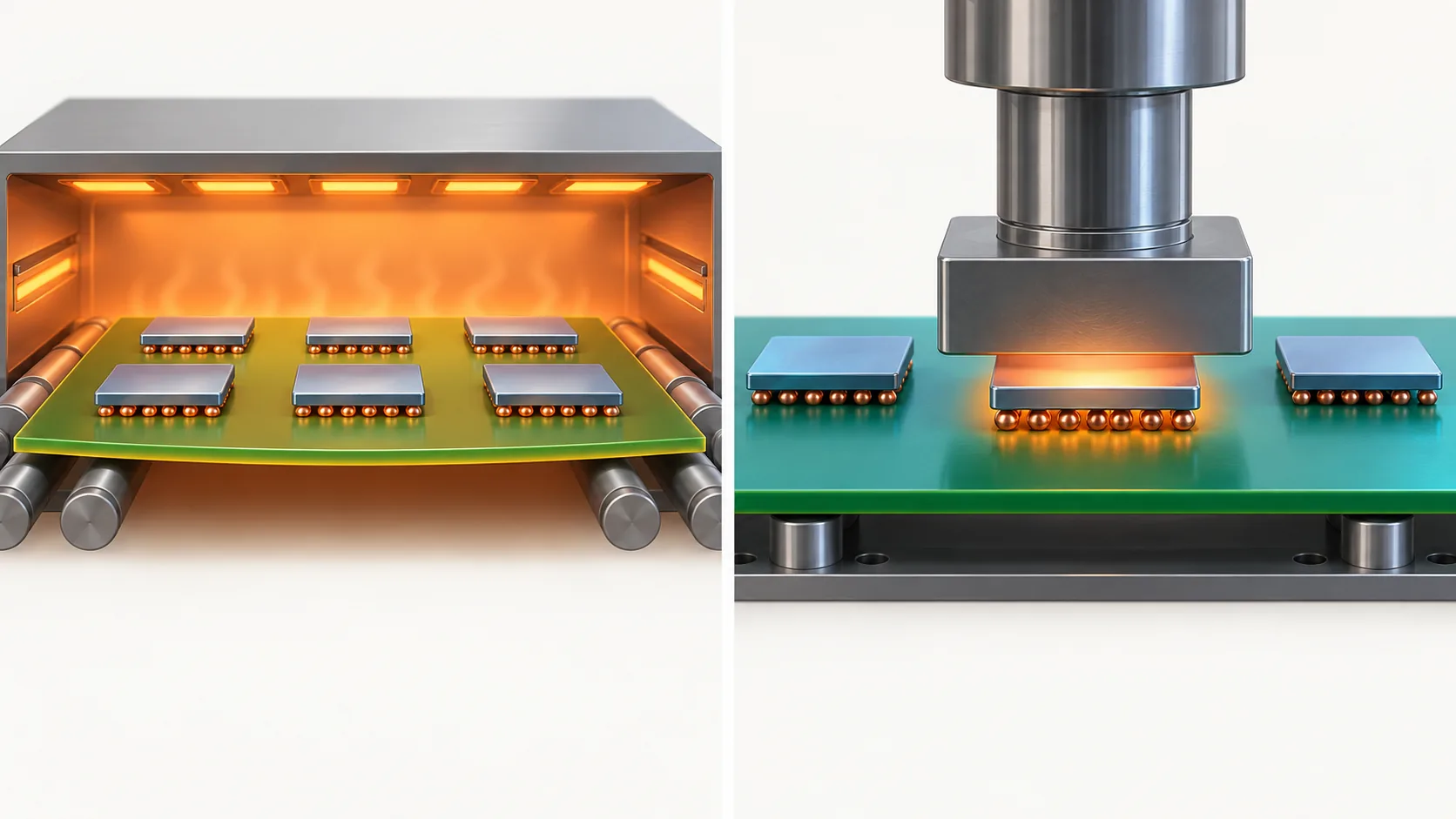
(1) Bake them all at once, or press one at a time
There are broadly two ways to make flip chip joints. In describing its own packages, Amkor notes that fine-pitch flip chip connections are made by either "thermocompression with non-conductive paste (TCNCP) or mass reflow with capillary underfill (CUF)"Sourced.