TECHNOLOGY EXPLAINER
What a Chiplet Is
— why the industry gave up on one big chip and started splitting it apart
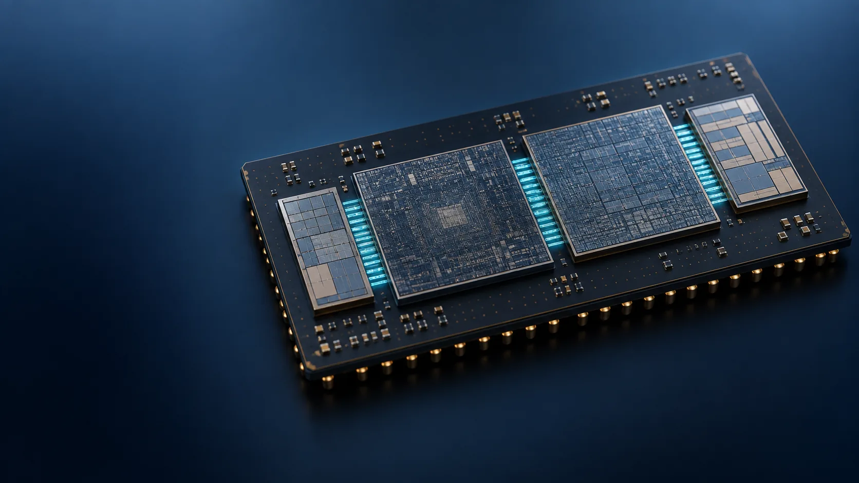
For decades the direction of travel in semiconductors was clear: put everything on a single piece of silicon. That assumption is now breaking down. This article explains the shift from integration to deliberate division — written both for readers meeting the idea for the first time and for materials engineers who have to make it work.
- What a chiplet is (the short version)
- Why it became necessary
- The yield arithmetic that makes splitting pay
- Four ways to connect: substrate, bridge, interposer, 3D stack
- UCIe — a common standard for chiplets
- A materials engineer's view: ABF, underfill, warpage, heat
- Real products
- What is still hard: test, partitioning, heat
- What comes next (glass substrates, UCIe-3D)
- Glossary / Primary sources / Claim-to-source audit
Sourced = a value stated in published material from a research institute or manufacturer (link given)
Our calculation = a figure this article derived, with the assumptions spelled out
Not yet confirmed = research-stage work with no confirmed production record
1. What a chiplet is (the short version)
A chiplet is a function that would once have been built into a single chip, made instead as several smaller dies and reconnected inside one package.
- Split: compute, input/output and memory are manufactured as separate dies, one per role
- Choose: each die can use the process node that suits it. Nothing forces every block onto the newest node
- Connect: inside the package the dies are joined densely, across distances of a few to a few hundred micrometres
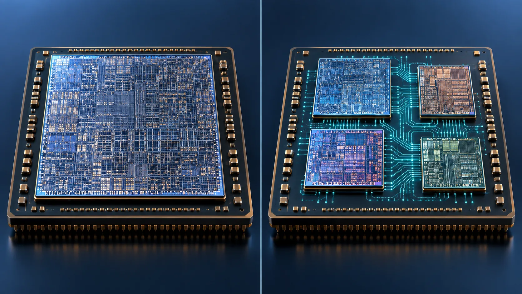
The neighbouring term is SoC, system-on-chip. An SoC is the idea of putting everything on one piece of silicon; a chiplet design deliberately splits the silicon and integrates in the package instead. The two are less opposites than a change of address: the point of integration has moved off the die and onto the package.
2. Why it became necessary
Reason 1: the chip cannot get any bigger — the reticle limit
Chips are made by projecting the image of a mask onto the wafer with a lithography scanner. There is a ceiling on the area that can be transferred in one exposure, and that ceiling is the reticle limit. In its description of CoWoS, TSMC uses one reticle, about 830 mm², as the yardstick for interposer areaSourced (TSMC).
However clever the design, then, a single die cannot be built much larger than roughly 800 to 860 mm². The compute that an AI accelerator is asked to deliver no longer fits inside that budget.
Reason 2: bigger dies yield worse
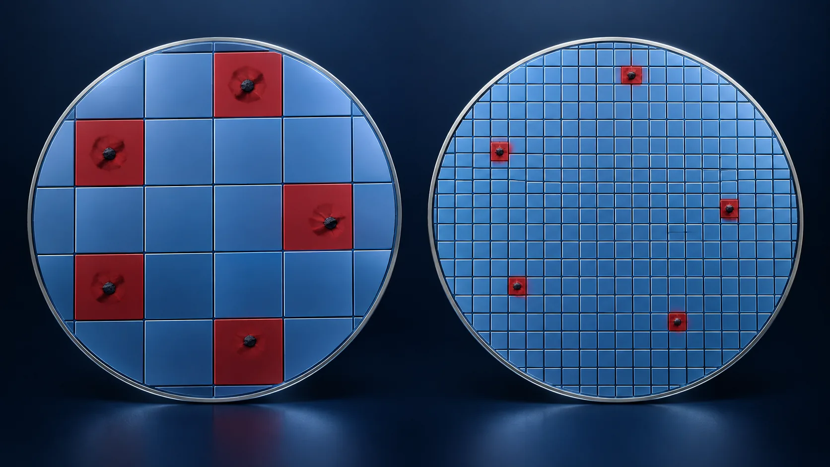
Defects land on the wafer at random. The larger a die, the likelier it is to catch one. Double the area and the failure rate roughly more than doubles — and a single microscopic defect throws away 800 mm² of silicon. The next section puts numbers on this.
Reason 3: there is no point building everything on the newest node
Shrinking to a leading-edge process mainly pays off for logic. Input/output and analogue circuits, which talk to the world outside, do not shrink in proportion and gain little in performance. On a monolithic SoC, though, those low-benefit circuits are still built at the leading-edge price per square millimetre.
AMD describes its EPYC processors as using a modular design that separates the compute dies from the input/output dieSourced (AMD). Being able to pick a process per role is where the money is.
The reticle limit says you cannot go bigger. Yield says going bigger throws away more. Economics says there is no need to build all of it at the leading edge. Because all three arrived at once, splitting the design stopped being a compromise and became the rational answer. That is the background to chiplets.
3. The yield arithmetic that makes splitting pay
Rather than leave this at the level of intuition, let us calculate. We use the simplest model available, the Poisson model.
Everything below is Our calculation. The defect density D = 0.1 per cm² is a value this article assumed, not a published figure from any foundry. Real yield models are more involved than Poisson (the Murphy model, for instance), and no manufacturer publishes its defect density. Read the trend with area, not the absolute numbers.
Compare the silicon consumed per good part
A common misreading is that splitting the design raises yield and that is the saving. That is only half true. Split 800 mm² into four dies of 200 mm² and the probability that all four are good is 0.82 to the fourth power, about 0.45 — exactly where the monolithic die started.
The real difference is how much you throw away when something fails. With chiplets you can gather only the good dies and build from those.
| Approach | Die area | Yield | Silicon consumed per good part |
|---|---|---|---|
| Monolithic (one big die) | 800 mm² | 44.9% | 17.8 cm² |
| Chiplets (200 mm² × 4) | 200 mm² × 4 | 81.9% (per die) | 9.8 cm² |
Both rows are Our calculation. Silicon consumed = area divided by yield. The chiplet row is 2 cm² divided by 0.819, times four dies.
The silicon needed to ship one of the same product falls from 17.8 cm² to 9.8 cm², roughly 45% less. That is the economic case for chiplets.
Splitting the design creates costs that did not exist before: the wiring layer or interposer that links the dies, the cost of testing every die before assembly (known good die), the circuits and power burned on die-to-die traffic, and the yield loss that comes with a physically larger package. The 45% above is strictly what you see when you look at silicon area and nothing else.
4. Four ways to connect: substrate, bridge, interposer, 3D stack
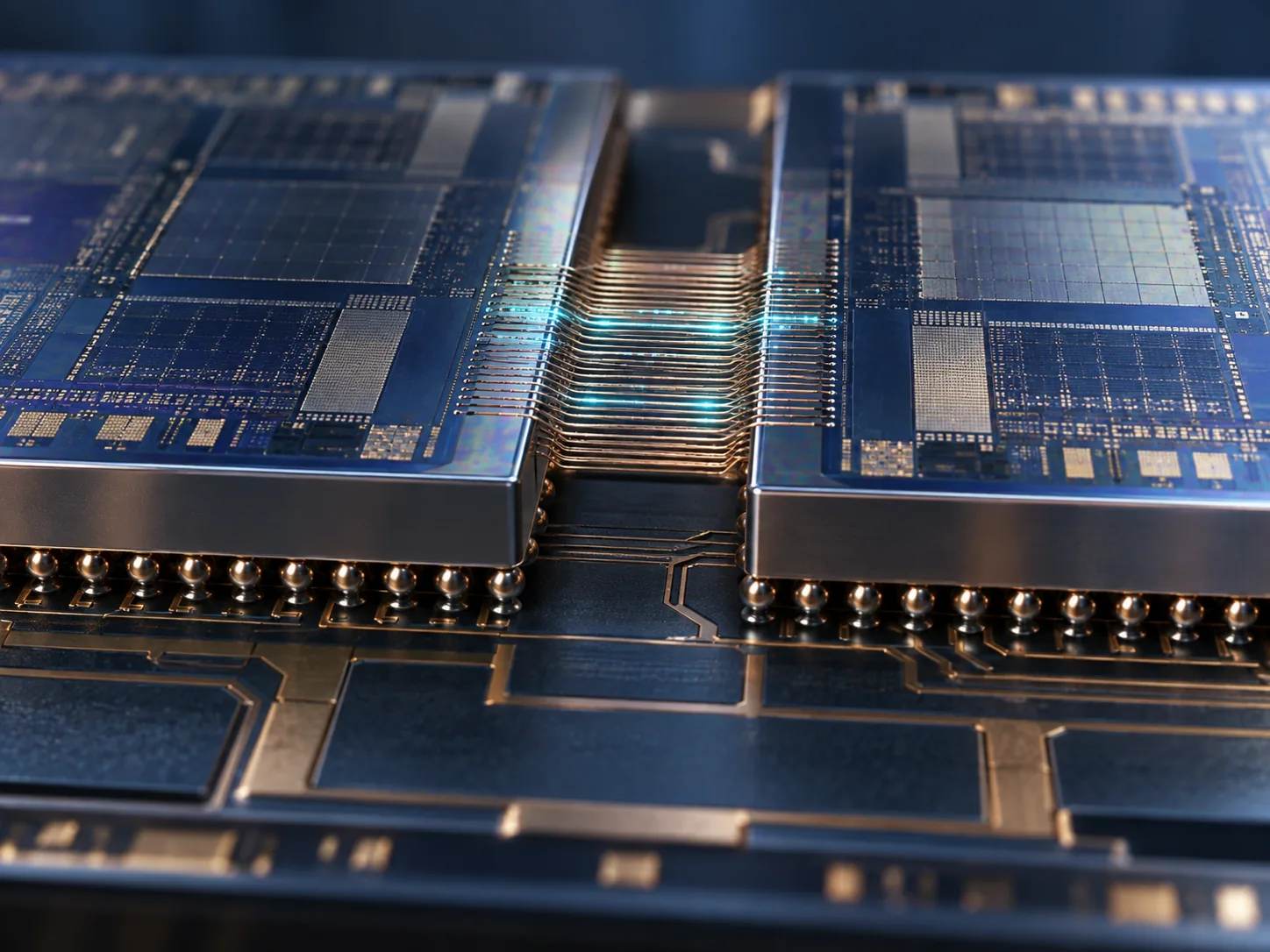
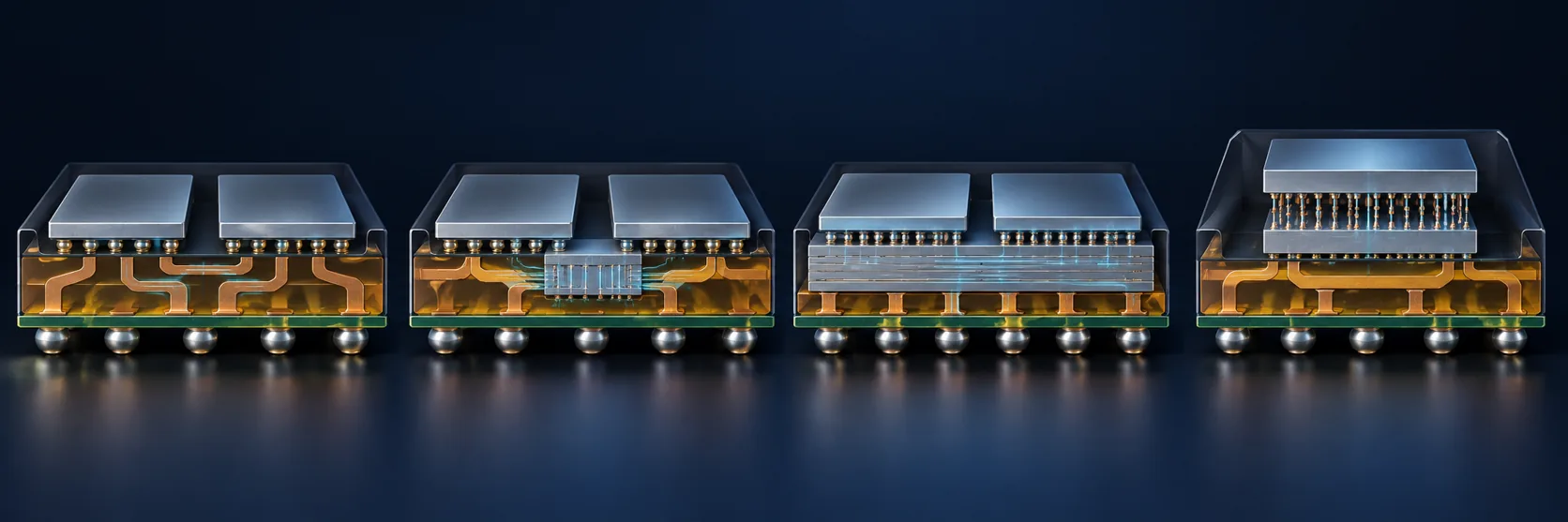
Strip the topic back and the technical content of chiplets comes down to one question: how finely can two dies be joined? Fineness is expressed as bump pitch, the spacing between connection points.
| Approach | Representative example | Bump pitch | Character | Source |
|---|---|---|---|---|
| (a) Direct on an organic substrate | UCIe Standard Package profile | 100–130 µm | Reach of 10 to 25 mm. Cheapest, but the wire count is limited | UCIe |
| (b) Silicon bridge | Intel EMIB (second generation) | 55 µm → 45 µm | A small piece of silicon is embedded only where the substrate needs it | Intel |
| (c) Interposer | TSMC CoWoS / UCIe Advanced Package profile | 25–55 µm | Reach under 2 mm. Silicon across the whole area, so the area cost is large | UCIe / TSMC |
| (d) 3D stacking (hybrid bonding) | Intel Foveros Direct 3D / TSMC SoIC | 10 µm and below | Copper bonded directly with no solder. Up to ten times the density of the earlier approach | Intel / TSMC |
All rows are Sourced; see the reference list at the end. Intel describes Foveros Direct 3D as giving up to ten times the interconnect density of conventional microbumps.
5. UCIe — a common standard for chiplets
Chiplets run into one more wall: a die from another company will not connect. As long as every vendor uses its own private link, chiplets stay an in-house affair.
UCIe (Universal Chiplet Interconnect Express) was written to solve exactly that. It standardises the physical layer, the protocol and the software stack for die-to-die links. The consortium was announced on 2 March 2022 together with the UCIe 1.0 specificationSourced.
| Release | Announced | What it added |
|---|---|---|
| UCIe 1.0 | March 2022 | Standardised the physical layer, protocol, software model and compliance testing for die-to-die links |
| UCIe 1.1 | August 2023 | A new bump map, extending support to lower-cost packages |
| UCIe 2.0 | August 2024 | Support for 3D packaging. Data rate of 32 GT/s |
| UCIe 3.0 | August 2025 | Doubled to 48 and 64 GT/s. Sideband reach extended to as much as 100 mm |
All rows are Sourced (UCIe Consortium announcements).
Three package profiles
UCIe defines three profiles, one per assembly styleSourced.
| Profile | Bump pitch | Reach | Data lanes |
|---|---|---|---|
| Standard Package (UCIe-S) | 100–130 µm | 10–25 mm | 16 |
| Advanced Package (UCIe-A) | 25–55 µm | under 2 mm | 64 |
| UCIe-3D | 10–25 µm down to 1 µm and below | Stacked (3D) | — |
If UCIe takes hold, putting company A's compute die and company B's input/output die in the same package becomes a practical option. It helps to think of it as trying to do inside the package what PCI Express does on the board.
6. A materials engineer's view: ABF, underfill, warpage, heat
Read all of the above from the materials side and chiplets become a technology that asks substrate, joining and encapsulation materials for a level of performance nobody needed before.
(1) Package substrate — ABF, a key material that came out of Japan
The interlayer dielectric in the organic substrate that carries the chiplets is, in practice, a single material: ABF, Ajinomoto Build-up Film. Ajinomoto says it was adopted by a major semiconductor manufacturer in 1999 and is now used in close to 100% of mainstream personal computersSourced (Ajinomoto).
As a material it is a formulation of epoxy resin, hardener and inorganic filler, and the company describes it as allowing circuits at micrometre scale to be formed by laser drilling and copper plated directly onto the surfaceSourced.
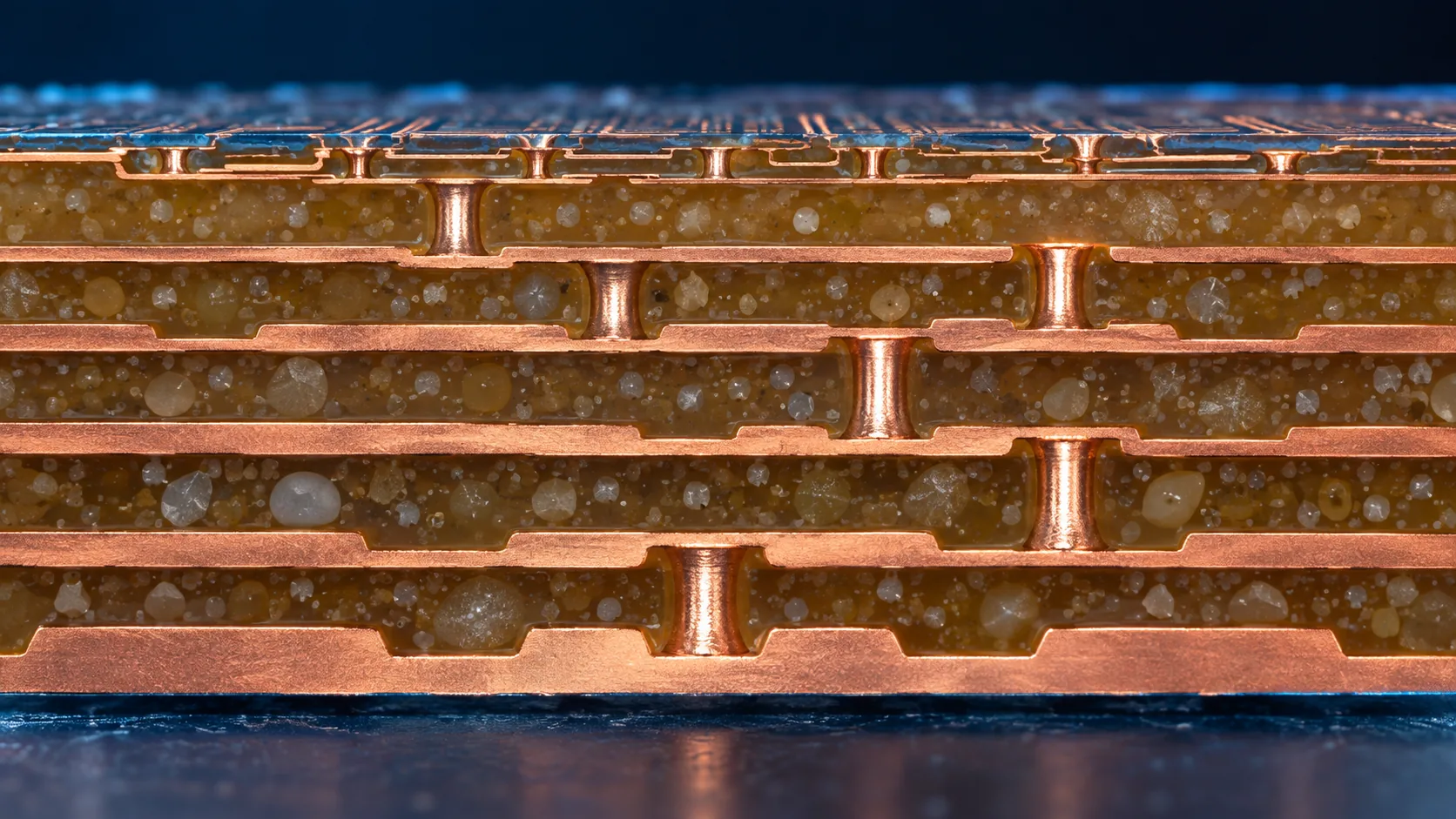
The dielectric is being pulled in three directions at once. (a) Finer wiring wants smaller filler particles and a smoother resin surface. (b) Plating adhesion wants a roughened surface — head-on conflict with (a). (c) High-speed signalling wants lower permittivity and loss tangent, yet the lowest-loss resins tend to be the worst for adhesion and heat resistance.
On top of that sits (d) low warpage and low thermal expansion over a large area. The larger the package grows with chiplet integration, the harsher these simultaneous conditions become. What limits chiplets is often not the silicon but the substrate material.
(2) Underfill — the physical wall that finer pitch puts in front of you
The gap between die and substrate is filled with underfill resin to relieve stress and protect the bumps. But the finer the bump pitch, the narrower the gap, and the less willing the resin is to flow in by capillary action. Any void left behind becomes a break in the thermal path and a starting point for delamination.
Seen from the materials side, the march from 100 µm pitch down towards 10 µm and below (Fig. 6) is also the process by which flow-in filling stops being usable. Hybrid bonding is moving towards direct copper joints without solder bumps not only for performance, but because this filling limit is closing in behind it.
(3) Warpage — growing the package feeds it directly
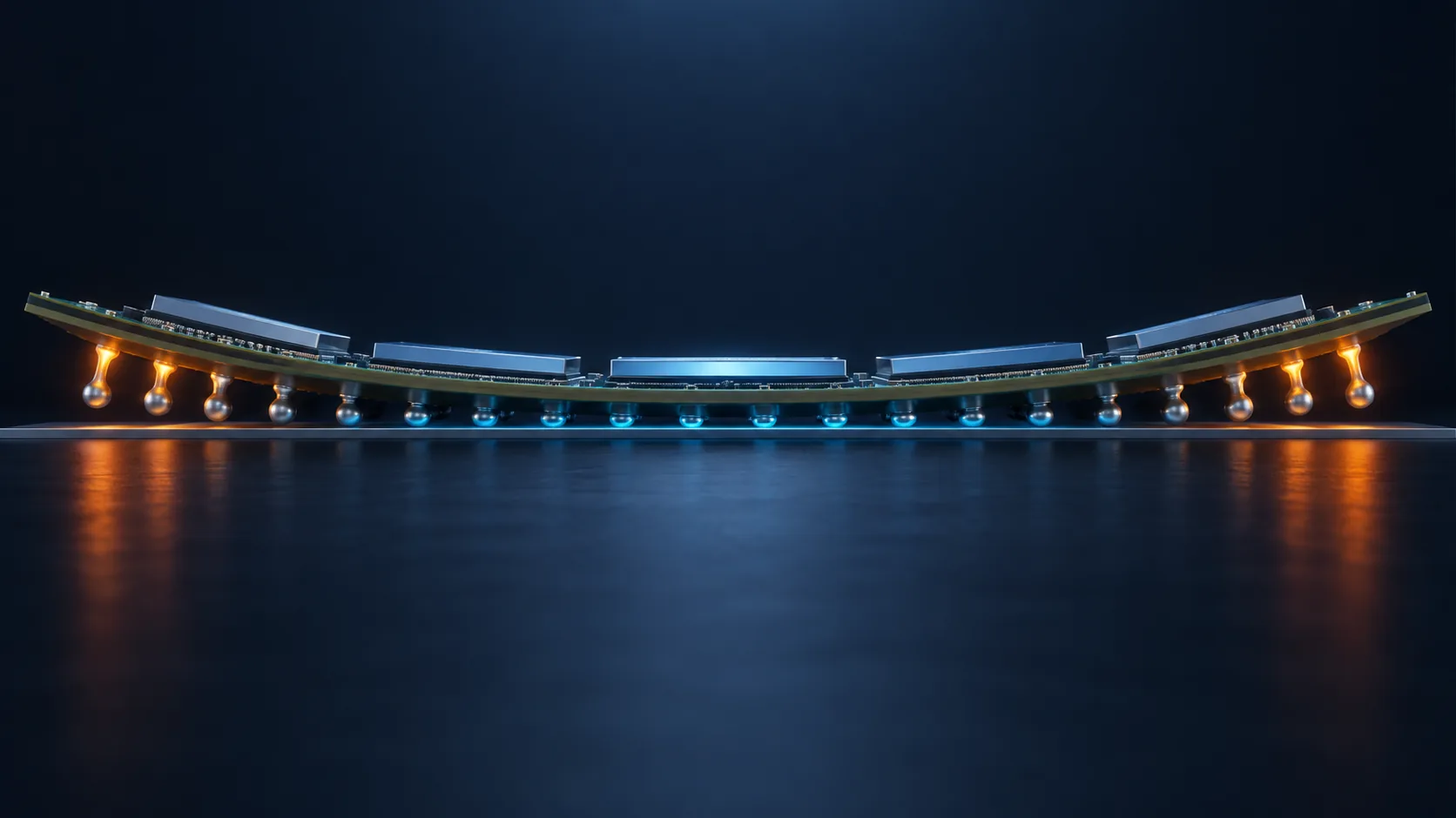
Chiplets make packages larger. Silicon, copper, epoxy resin and the organic substrate all have different coefficients of thermal expansion, so every heating and cooling cycle produces warpage. Warpage grows roughly in proportion to package dimensions, which means a larger package makes the problem worse by construction.
Intel says of its glass substrates that they dramatically reduce the warpage problem that constrains conventional organic substrate solutionsSourced. Turn that around and the manufacturer is conceding that warpage is one of the rate-limiting factors in organic substrates today.
(4) Heat — every die has its own power density
Unlike a monolithic SoC, a chiplet package holds dies with very different power densities side by side. The compute dies run hot while the input/output die stays comparatively cool, and that temperature gradient makes the in-plane stress distribution more complicated still. Thickness variation in the thermal interface material, and how to absorb differences in die height, land on the assembly-materials side as well.
7. Real products
| When | Product | Published configuration |
|---|---|---|
| August 2019 | AMD second-generation EPYC (7002 series) | A chiplet design carrying up to 64 "Zen 2" cores built on a 7 nm process |
| — | AMD EPYC (current generation) | A modular design separating the compute dies (CCD) from the input/output die (IOD), linked by Infinity Fabric |
| — | Intel Data Center GPU Max series | EMIB 3.5D, combining EMIB with Foveros. More than 100 billion transistors, 47 active tiles and five process nodes |
All rows are Sourced (AMD and Intel publications).
Intel's "47 tiles, five nodes" is the clearest statement of where the chiplet idea ends up. One product made of 47 parts built on five different manufacturing processes — that is no longer a chip. It is a system mounted on a board that happens to be called a package.
8. What is still hard: test, partitioning, heat
(1) Test — can you tell a good die before you build with it?
The advantage of chiplets was that you can gather only the good dies. Inverted, that says the advantage does not exist at all unless every die can be judged reliably before assembly. Build in one bad die and the whole package is wasted, good dies included. The more dies and the more tiers, the more exacting this judgement has to be.
(2) Partitioning — where to draw the line
Which function goes on which die touches performance, cost and power alike. Traffic that crosses a die boundary is slower than wiring inside one die, and it burns more power. Split too finely and the communication overhead eats the benefit.
(3) Heat and mechanical stress
As set out in section 6. Larger packages, denser integration and uneven heat all arrive together, so it is increasingly the materials and the structure that set the performance ceiling.
9. What comes next
Glass substrates: in September 2023 Intel announced glass substrates for next-generation advanced packagingSourced. It cites the potential for ten times the interconnect density, 50% less pattern distortion, ultra-flatness that helps lithographic depth of focus, and a large reduction in warpage, with a plan to bring the technology to market in the second half of this decade.
UCIe-3D: written around hybrid bonding, its scope reaches down to pitches of 1 µm and belowSourced.
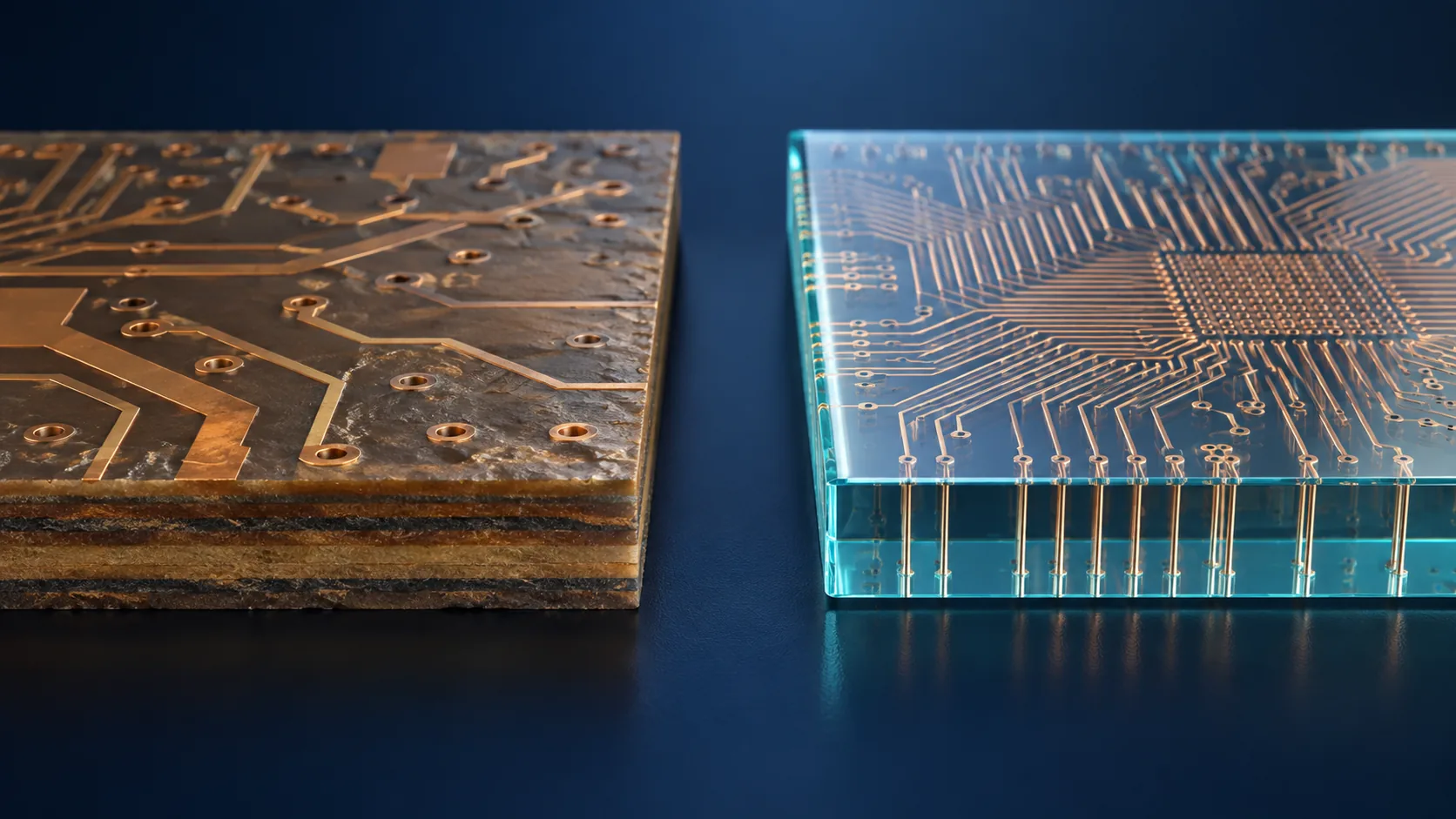
The production timing, yield and cost of glass substrates had not been published when this article was researchedNot yet confirmed. Nor is it settled whether hybrid bonding will replace organic substrate assembly or whether the two will coexist, each in its own applications. The important discipline is not to confuse a roadmap target with a production record.
10. Glossary
- Chiplet
- A small die holding part of the function. Several are integrated into one package.
- Monolithic
- The conventional approach of building every function into a single silicon die.
- Die
- An individual silicon chip cut from the wafer.
- Reticle limit
- The largest area a scanner can expose at once. It sets the ceiling on one die.
- Yield
- The share of manufactured parts that are good. It falls as die area grows.
- KGD
- Known good die. A die confirmed good before assembly.
- Bump pitch
- The spacing between connection points. Finer pitch carries more wires.
- UCIe
- Universal Chiplet Interconnect Express. The industry standard for die-to-die links.
- EMIB
- Intel's approach, embedding a silicon bridge only where the organic substrate needs one.
- Foveros
- Intel's 3D stacking technology. Foveros Direct 3D uses hybrid bonding.
- CoWoS
- TSMC's 2.5D assembly technology, placing dies side by side on a silicon interposer.
- SoIC
- TSMC's 3D stacking technology. Bonding without bumps, with pitches starting under 10 µm.
- Interposer
- The intermediate substrate that carries the dies. A silicon one allows very many fine connections.
- ABF
- Ajinomoto Build-up Film. The interlayer dielectric of the package substrate.
- Underfill
- Resin filling the gap between die and substrate. It relieves stress and protects the bumps.
- Hybrid bonding
- Joining copper and dielectric directly, with no solder bumps.
11. Primary sources
- UCIe Consortium "Specifications" — uciexpress.org
- UCIe Consortium "UCIe Consortium Introduces 3.0 Specification With 64 GT/s Performance and Enhanced Manageability", 5 August 2025 — businesswire.com
- UCIe Consortium "UCIe Consortium Releases 2.0 Specification Supporting Manageability System Architecture and 3D Packaging", 6 August 2024 — businesswire.com
- UCIe Consortium "UCIe Consortium Releases its 1.1 Specification", 8 August 2023 — businesswire.com
- UCIe Consortium "Leaders in Semiconductors, Packaging, IP Suppliers, Foundries, and Cloud Service Providers Join Forces to Standardize Chiplet Ecosystem", 2 March 2022 — businesswire.com
- Intel "Advanced Packaging Innovations" — intel.com
- Intel "Foveros Direct 3D Technology Brief" — intel.com (PDF)
- Intel "Intel Unveils Industry-Leading Glass Substrates to Meet Demand for More Powerful Compute", September 2023 — newsroom.intel.com
- Intel "In Glass, a View to the Future of Powerful Chips", 16 November 2023 — newsroom.intel.com
- TSMC "CoWoS" technology page — 3dfabric.tsmc.com
- TSMC "TSMC-SoIC" technology page — 3dfabric.tsmc.com
- AMD "2nd Gen AMD EPYC Processors Set New Standard for the Modern Datacenter", 7 August 2019 — ir.amd.com
- AMD "AMD EPYC Server CPUs Features and Technologies" — amd.com
- Ajinomoto "ABF" innovation story (Japanese-language page) — ajinomoto.co.jp
12. Claim-to-source audit
| Claim in the text | Basis | Label |
|---|---|---|
| Interposer area is measured against one reticle, about 830 mm² | TSMC CoWoS technology page[Source 10] https://3dfabric.tsmc.com/english/dedicatedFoundry/technology/cowos.htm | Sourced |
| The yield curve; 200 mm² giving about 82% and 800 mm² about 45%; silicon consumed falling from 17.8 to 9.8 cm² | Our calculation from Y = exp(−D × A) with an assumed D of 0.1 per cm². Not a measured figure | Our calculation |
| AMD EPYC uses a modular design separating the compute dies from the input/output die | AMD technology page[Source 13] https://www.amd.com/en/products/processors/server/epyc/technology-leadership.html | Sourced |
| AMD second-generation EPYC (7 August 2019) carries up to 64 Zen 2 cores built on 7 nm | AMD press release[Source 12] https://ir.amd.com/news-events/press-releases/detail/904/2nd-gen-amd-epyc-processors-set-new-standard-for-the-modern-datacenter-with-record-breaking-performance-and-significant-tco-savings | Sourced |
| UCIe Standard Package at 100–130 µm, 10–25 mm and 16 lanes; Advanced at 25–55 µm, under 2 mm and 64 lanes; UCIe-3D from 10–25 µm down to 1 µm and below | UCIe Consortium specifications page[Source 1] https://www.uciexpress.org/specifications | Sourced |
| UCIe 1.0 (March 2022), 1.1 (August 2023), 2.0 (August 2024, 32 GT/s) and 3.0 (August 2025, 48 and 64 GT/s, sideband to 100 mm) | UCIe Consortium press releases[Source 2] https://www.businesswire.com/news/home/20250805909613/en/UCIe-Consortium-Introduces-3.0-Specification-With-64-GTs-Performance-and-Enhanced-Manageability[Source 3] https://www.businesswire.com/news/home/20240806155624/en/UCIe-Consortium-Releases-2.0-Specification-Supporting-Manageability-System-Architecture-and-3D-Packaging[Source 4] https://www.businesswire.com/news/home/20230808798613/en/UCIe-Universal-Chiplet-Interconnect-Express-Consortium-Releases-its-1.1-Specification[Source 5] https://www.businesswire.com/news/home/20220302005254/en | Sourced |
| Second-generation Intel EMIB moves bump pitch from 55 µm to 45 µm | Intel publication[Source 6] https://www.intel.com/content/www/us/en/foundry/packaging.html | Sourced |
| Foveros Direct 3D works below 10 µm pitch and gives up to ten times the interconnect density of conventional microbumps | Intel Foveros Direct 3D technology brief[Source 7] https://www.intel.com/content/dam/www/central-libraries/us/en/documents/2025-11/foveros-direct-3d-tech-brief.pdf | Sourced |
| Intel Data Center GPU Max: more than 100 billion transistors, 47 active tiles, five process nodes, EMIB 3.5D | Intel publication[Source 6] https://www.intel.com/content/www/us/en/foundry/packaging.html | Sourced |
| TSMC SoIC bond pitches start below 10 µm | TSMC SoIC technology page[Source 11] https://3dfabric.tsmc.com/english/dedicatedFoundry/technology/SoIC.htm | Sourced |
| ABF was adopted in 1999 and is used in close to 100% of mainstream personal computers; it combines epoxy resin, hardener and inorganic filler; laser drilling and direct copper plating form micrometre-scale circuits | Ajinomoto published page[Source 14] https://www.ajinomoto.co.jp/company/jp/rd/our_innovation/abf/ | Sourced |
| Glass substrates: potential for ten times the interconnect density, 50% less pattern distortion, a large reduction in warpage, and market entry in the second half of this decade | Intel announcement of September 2023 and the related article[Source 8] https://newsroom.intel.com/artificial-intelligence/intel-unveils-industry-leading-glass-substrates[Source 9] https://newsroom.intel.com/new-technologies/in-glass-view-future-of-powerful-chips | Sourced |
| That smoothness and adhesion pull the dielectric in opposite directions, that underfill flow has a filling limit, and that warpage worsens in proportion to package size | Commentary based on general relationships in materials engineering. No specific numerical claim is made | Commentary |
| The production timing, yield and cost of glass substrates, and how widely hybrid bonding will be adopted | No publication could be confirmed at the time this article was researched | Not yet confirmed |
Last updated 20 September 2026. Sources are limited to primary material (publications from the standards body and official announcements and technology pages from manufacturers). All figures are explanatory concept graphics. Visual-overview figures are shown as AI-generated conceptual images, matching the Japanese edition. Vector drawings are retained where they carry quantitative values or precision-critical technical labels. AI-generated images do not depict real equipment, products, facilities, dimensions or exact cross-sections; replaced source SVG overview drawings remain in the HTML but are hidden.